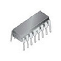
TC74HC4538AP Toshiba, TC74HC4538AP Datasheet

TC74HC4538AP
Specifications of TC74HC4538AP
Available stocks
Related parts for TC74HC4538AP
TC74HC4538AP Summary of contents
Page 1
... V more than 1 k Ω 28% V (min) NIL (min ∼ − t pLH pHL (opr GND TC74HC4538AP/AF/AFN/AFT Note: The JEDEC SOP (FN) is not available in Japan. TC74HC4538AP TC74HC4538AF TC74HC4538AFN TC74HC4538AFT Weight DIP16-P-300-2.54A : 1.00 g (typ.) SOP16-P-300.1.27A : 0.18 (typ.) SOL16-P-150-1.27 : 0.13 g (typ.) TSSOP16-P-0044-0.65A : 0.06 g (typ. 2007-10-01 ...
Page 2
... Pin Assignment 1T1 1 1T2 GND 8 (top view) Truth Table Inputs Outputs Don’t care IEC Logic Symbol 2T1 1 CD 1T1 14 2T2 1T2 (12) 2A (11 (13 (15 2T1 (14) 2T2 Note Output Enable Inhibit Inhibit Output Enable Reset 2 TC74HC4538AP/AF/AFN/AFT (4) & (5) (6) 1Q (3) R ( & (10 ( 2007-10-01 ...
Page 3
... In the care of a system that does not satisfy the above condition, an external clamping diode is needed to protect the IC from rush current level in the wait state, i.e. when no trigger is applied. Supply CC is discharged mainly through the internal (parasitic) diode the limitation of fall time of the supply voltage is determined as follows TC74HC4538AP/AF/AFN/AFT sufficiently X drops slowly, the rush current is CC 2007-10-01 ...
Page 4
... System Diagram Timing Chart wOUT V L ref F/F t wOUT 4 TC74HC4538AP/AF/AFN/AFT V H ref wOUT rr 2007-10- ref V L ref GND ...
Page 5
... X X · The voltage level of T2 then falls trigger, t (min), depends TC74HC4538AP/AF/AFN/AFT start operating, and Q is turned on. The 2 N becomes low. The flip-flop is then 1 continues operating the IC returns to ref ), is as follows: wOUT L level again. ...
Page 6
... Note 1: The operating ranges must be maintained to ensure the normal operation of the device. Unused inputs must be tied to either VCC or GND. Note 2: The maximum allowable values of C TC74HC4538A, and leakage due to board layout and surface resistance. Susceptibility to externally induced noise signals may occur for R TC74HC4538AP/AF/AFN/AFT Symbol Rating V −0 ...
Page 7
... GND 6 GND 6 GND 6 2 GND IN CC 4.5 T2 ext = 0 6.0 7 TC74HC4538AP/AF/AFN/AFT Ta = − 25°C 85°C Min Typ. Max Min Max 1.50 ― ― 1.50 ― 3.15 ― ― 3.15 ― 4.20 ― ― 4.20 ― ― ― 0.50 ― 0.50 ― ― 1.35 ― ...
Page 8
... Timing Requirements (input: t Characteristics Symbol Minimum pulse width ( Minimum clear width ( CD ) Minimum clear removal time Minimum retrigger time AC Characteristics ( pF Characteristics Symbol Output transition time Propagation delay time ( Propagation delay time ( CD - TC74HC4538AP/AF/AFN/AFT = ns Test Condition t w (L) ― (H) t ― w (L) t ― rem kΩ ...
Page 9
... PD current consumption without load. Average operating current can be obtained by the equation ·V ·f CC (opr active supply current) CC’ (duty: %) TC74HC4538AP/AF/AFN/AFT = ns Test Condition V (V) CC 2.0 ― 4.5 6.0 2.0 ― ...
Page 10
... X wOUT 0.9 0 0.01 μ 0.1 μF 0 μ Supply voltage V ( – C Characteristics (typical) wOUT 4 MΩ 100 kΩ kΩ kΩ 1 − External capacitor C (pF) X TC74HC4538AP/AF/AFN/AFT = K·C · 0 – V Characteristics (typical 25° 0.01 μ 1000 100 Supply voltage V (V) CC 2007-10-01 ...
Page 11
... Package Dimensions Weight: 1.00 g (typ.) TC74HC4538AP/AF/AFN/AFT 11 2007-10-01 ...
Page 12
... Package Dimensions Weight: 0.18 g (typ.) TC74HC4538AP/AF/AFN/AFT 12 2007-10-01 ...
Page 13
... Package Dimensions (Note) Note: This package is not available in Japan. Weight: 0.13 g (typ.) TC74HC4538AP/AF/AFN/AFT 13 2007-10-01 ...
Page 14
... Package Dimensions Weight: 0.06 g (typ.) TC74HC4538AP/AF/AFN/AFT 14 2007-10-01 ...
Page 15
... Please contact your TOSHIBA sales representative for details as to environmental matters such as the RoHS compatibility of Product. Please use Product in compliance with all applicable laws and regulations that regulate the inclusion or use of controlled substances, including without limitation, the EU RoHS Directive. TOSHIBA assumes no liability for damages or losses occurring as a result of noncompliance with applicable laws and regulations. TC74HC4538AP/AF/AFN/AFT 15 2007-10-01 ...


