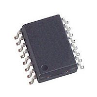
TC74HC123AF Toshiba, TC74HC123AF Datasheet

TC74HC123AF
Specifications of TC74HC123AF
Available stocks
Related parts for TC74HC123AF
TC74HC123AF Summary of contents
Page 1
... In the case of using only one circuit, CLR should be tied to GND, Rx/Cx・Cx・Q・ Q should be tied to OPEN, the other inputs should be tied to V MOS 28% V (min) NIL (min ∼ − t pLH pHL (opr GND TC74HC123AP/AF/AFN Note: xxxFN (JEDEC SOP) is not available in Japan. TC74HC123AP TC74HC123AF TC74HC123AFN Weight DIP16-P-300-2.54A : 1.00 g (typ.) SOP16-P-300-1.27A : 0.18 g (typ.) SOL16-P-150-1.27 : 0.13 g (typ.) 2007-10-01 ...
Page 2
Pin Assignment IEC Logic Symbol TC74HC123AP/AF/AFN 2 2007-10-01 ...
Page 3
Block Diagram (Note 1)(Note 2) Note 1: Cx, Rx, Dx are external capacitor, resistor, and diode, respectively. Note 2: External clamping diode, Dx; The external capacitor is charged the supply voltage is turned off discharges ...
Page 4
System Diagram CLR Timing Chart V ref F TC74HC123AP/AF/AFN V ref ...
Page 5
Functional Description (1) Stand-by state The external capacitor (Cx) is fully charged to V triggering, the Q and Q P comparators that relate to the timing of the output pulse, and two reference voltage supplies turn off. The total supply ...
Page 6
... Please design the appropriate reliability upon reviewing the Toshiba Semiconductor Reliability Handbook (“Handling Precautions”/“Derating Concept and Methods”) and individual reliability data (i.e. reliability test report and estimated failure rate, etc). Note 2: 500 mW in the range − ...
Page 7
Electrical Characteristics DC Characteristics Characteristics Symbol High-level input V IH voltage Low-level input V IL voltage High-level output voltage Low-level output voltage Input leakage I IN current Rx/Cx terminal I ...
Page 8
Timing Requirements (input: t Characteristics Symbol Minimum pulse width Minimum clear width Minimum retrigger time AC Characteristics = 15 pF Characteristics Output transition time Propagation delay time ( Propagation delay time ( ...
Page 9
AC Characteristics = 50 pF, input Characteristics Symbol t TLH Output transition time t THL Propagation delay t pLH time t pHL ( Propagation delay time t pLH ( CLR TRIGGER-Q, t ...
Page 10
Output Pulse Width Constant K – Supply Voltage (typical) t – Cx Characteristics (typ.) WOUT TC74HC123AP/AF/AFN t – V Characteristics (typ 2007-10-01 ...
Page 11
Package Dimensions Weight: 1.00 g (typ.) TC74HC123AP/AF/AFN 11 2007-10-01 ...
Page 12
Package Dimensions Weight: 0.18 g (typ.) TC74HC123AP/AF/AFN 12 2007-10-01 ...
Page 13
Package Dimensions (Note) Note: This package is not available in Japan. Weight: 0.13 g (typ.) TC74HC123AP/AF/AFN 13 2007-10-01 ...
Page 14
... Product shall not be used for or incorporated into any products or systems whose manufacture, use, or sale is prohibited under any applicable laws or regulations. • The information contained herein is presented only as guidance for Product use. No responsibility is assumed by TOSHIBA for any infringement of patents or any other intellectual property rights of third parties that may result from the use of Product. No license to any intellectual property right is granted by this document, whether express or implied, by estoppel or otherwise. • ...


