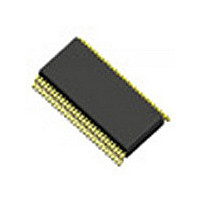
74ALVCHR162269APAG8 IDT, Integrated Device Technology Inc, 74ALVCHR162269APAG8 Datasheet - Page 3

74ALVCHR162269APAG8
Manufacturer Part Number
74ALVCHR162269APAG8
Description
Manufacturer
IDT, Integrated Device Technology Inc
Datasheet
1.74ALVCHR162269APAG8.pdf
(7 pages)
Specifications of 74ALVCHR162269APAG8
Lead Free Status / RoHS Status
Compliant
PIN DESCRIPTION
NOTE:
1. These pins have "Bus-Hold". All other pins are standard inputs, outputs, or I/Os.
DC ELECTRICAL CHARACTERISTICS OVER OPERATING RANGE
Following Conditions Apply Unless Otherwise Specified:
Operating Condition: T
NOTE:
1. Typical values are at V
Pin Names
IDT74ALVCH162269A
3.3V CMOS 12-BIT TO 24-BIT REGISTERED BUS EXCHANGER
CLKENA1
CLKENA2
1Bx
2Bx
Symbol
Ax
OEB1
OEB2
OEA
CLK
SEL
∆I
I
I
I
I
I
V
V
OZH
V
CCH
CCZ
OZL
V
CCL
I
(1:12)
I
IH
(1:12)
(1:12)
IL
CC
IH
IL
IK
H
I/O
I/O
I/O
I/O
Input HIGH Voltage Level
Input LOW Voltage Level
Input HIGH Current
Input LOW Current
High Impedance Output Current
(3-State Output pins)
Clamp Diode Voltage
Input Hysteresis
Quiescent Power Supply Current
Quiescent Power Supply Current
Variation
I
I
I
I
I
I
I
Description
Bidirectional Data Port A. Usually connected to the CPU’s Address/Data bus.
Bidirectional Data Port 1B. Usually connected to the even path or even bank of memory.
Bidirectional Data Port 2B. Usually connected to the odd path or odd bank of memory.
Clock Input
Clock Enable Input for the A-1B Register. If CLKENA1 is LOW during the rising edge of CLK, data will be clocked into register A-1B (Active LOW).
Clock Enable Input for the A-2B Register. If CLKENA2 is LOW during the rising edge of CLK, data will be clocked into register A-2B (Active LOW).
1B or 2B Port Selection. When HIGH during the rising edge of CLK, SEL enables data transfer from 1B Port to A Port. When LOW during the rising
edge of CLK, SEL enables data transfer from 2B Port to A Port.
Synchronous Output Enable for A Port (Active LOW)
Synchronous Output Enable for 1B Port (Active LOW)
Synchronous Output Enable for 2B Port (Active LOW)
A
CC
= –40°C to +85°C
Parameter
= 3.3V, +25°C ambient.
V
V
V
V
V
V
V
V
V
V
V
One input at V
CC
CC
CC
CC
CC
CC
CC
CC
CC
CC
IN
= GND or V
= 2.3V to 2.7V
= 2.7V to 3.6V
= 2.3V to 2.7V
= 2.7V to 3.6V
= 2.3V, I
= 3.6V
= 3.6V
= 3.6V
= 3.3V
= 3.6V
IN
CC
= –18mA
CC
- 0.6V, other inputs at V
Test Conditions
3
V
V
V
V
I
I
O
O
= V
= GND
CC
= V
= GND
CC
or GND
CC
(1)
(1)
(1)
INDUSTRIAL TEMPERATURE RANGE
Min.
1.7
—
—
—
—
—
—
—
—
—
—
2
Typ.
–0.7
100
0.1
—
—
—
—
—
—
—
—
—
(1)
Max.
–1.2
±10
±10
750
0.7
0.8
±5
±5
—
—
—
40
Unit
µA
µA
µA
mV
µA
µA
V
V
V


