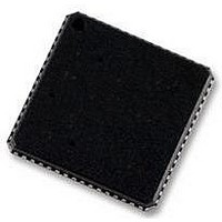
ADSP-BF592KCPZ Analog Devices Inc, ADSP-BF592KCPZ Datasheet - Page 8

ADSP-BF592KCPZ
Manufacturer Part Number
ADSP-BF592KCPZ
Description
58T4522
Manufacturer
Analog Devices Inc
Specifications of ADSP-BF592KCPZ
Operating Temperature (min)
0C
Operating Temperature (max)
70C
Operating Temperature Classification
Commercial
Mounting
Surface Mount
Pin Count
64
Rohs Compliant
YES
Frequency
400MHz
Embedded Interface Type
PPI, SPI, UART
No. Of I/o's
32
Operating Temperature Range
0°C To +70°C
Digital Ic Case Style
LFCSP
No. Of Pins
64
Core Supply Voltage
1.4V
Lead Free Status / RoHS Status
Compliant
Available stocks
Company
Part Number
Manufacturer
Quantity
Price
Company:
Part Number:
ADSP-BF592KCPZ-2
Manufacturer:
BROADCOM
Quantity:
154
ADSP-BF592
DMA CONTROLLERS
The processor has multiple, independent DMA channels that
support automated data transfers with minimal overhead for
the processor core. DMA transfers can occur between the pro-
cessor’s internal memories and any of its DMA-capable
peripherals. DMA-capable peripherals include the SPORTs, SPI
ports, UART, and PPI. Each individual DMA-capable periph-
eral has at least one dedicated DMA channel.
The processor DMA controller supports both one-dimensional
(1-D) and two-dimensional (2-D) DMA transfers. DMA trans-
fer initialization can be implemented from registers or from sets
of parameters called descriptor blocks.
The 2-D DMA capability supports arbitrary row and column
sizes up to 64K elements by 64K elements, and arbitrary row
and column step sizes up to ±32K elements. Furthermore, the
column step size can be less than the row step size, allowing
implementation of interleaved data streams. This feature is
especially useful in video applications where data can be de-
interleaved on the fly.
Examples of DMA types supported by the processor DMA con-
troller include:
In addition to the dedicated peripheral DMA channels, there are
two memory DMA channels, which are provided for transfers
between the various memories of the processor system with
minimal processor intervention. Memory DMA transfers can be
controlled by a very flexible descriptor-based methodology or
by a standard register-based autobuffer mechanism.
WATCHDOG TIMER
The processor includes a 32-bit timer that can be used to imple-
ment a software watchdog function. A software watchdog can
improve system availability by forcing the processor to a known
state through generation of a hardware reset, nonmaskable
interrupt (NMI), or general-purpose interrupt, if the timer
expires before being reset by software. The programmer initial-
izes the count value of the timer, enables the appropriate
interrupt, then enables the timer. Thereafter, the software must
reload the counter before it counts to zero from the pro-
grammed value. This protects the system from remaining in an
unknown state where software, which would normally reset the
timer, has stopped running due to an external noise condition
or software error.
If configured to generate a hardware reset, the watchdog timer
resets both the core and the processor peripherals. After a reset,
software can determine whether the watchdog was the source of
the hardware reset by interrogating a status bit in the watchdog
timer control register.
• A single, linear buffer that stops upon completion
• A circular, auto-refreshing buffer that interrupts on each
• 1-D or 2-D DMA using a linked list of descriptors
• 2-D DMA using an array of descriptors, specifying only the
full or fractionally full buffer
base DMA address within a common page
Rev. PrC | Page 8 of 46 | August 2010
The timer is clocked by the system clock (SCLK), at a maximum
frequency of f
TIMERS
There are four general-purpose programmable timer units in
the processors. Three timers have an external pin that can be
configured either as a pulse width modulator (PWM) or timer
output, as an input to clock the timer, or as a mechanism for
measuring pulse widths and periods of external events. These
timers can be synchronized: to an external clock input to the
several other associated PF pins, to an external clock input to
the PPI_CLK input pin, or to the internal SCLK.
The timer units can be used in conjunction with the UART to
measure the width of the pulses in the data stream to provide a
software auto-baud detect function for the respective serial
channels.
The timers can generate interrupts to the processor core provid-
ing periodic events for synchronization, either to the system
clock or to a count of external signals.
In addition to the three general-purpose programmable timers,
a fourth timer is also provided. This extra timer is clocked by the
internal processor clock and is typically used as a system tick
clock for generation of operating system periodic interrupts.
SERIAL PORTS
The processors incorporate two dual-channel synchronous
serial ports (SPORT0 and SPORT1) for serial and multiproces-
sor communications. The SPORTs support the following
features:
• I
• Bidirectional operation – Each SPORT has two sets of inde-
• Buffered (8-deep) transmit and receive ports – Each port
• Clocking – Each transmit and receive port can either use an
• Word length – Each SPORT supports serial data words
• Framing – Each transmit and receive port can run with or
• Companding in hardware – Each SPORT can perform
pendent transmit and receive pins, enabling eight channels
of I
has a data register for transferring data words to and from
other processor components and shift registers for shifting
data in and out of the data registers.
external serial clock or generate its own, in frequencies
ranging from (f
from 3 to 32 bits in length, transferred most-significant-bit
first or least-significant-bit first.
without frame sync signals for each data word. Frame sync
signals can be generated internally or externally, active high
or low, and with either of two pulse widths and early or late
frame sync.
A-law or μ-law companding according to ITU recommen-
dation G.711. Companding can be selected on the transmit
and/or receive channel of the SPORT without
additional latencies.
2
S capable operation.
2
S stereo audio.
SCLK
.
Preliminary Technical Data
SCLK
/131,070) Hz to (f
SCLK
/2) Hz.


