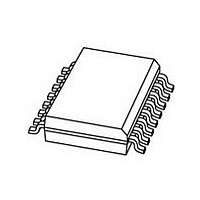
CBT3126DS NXP Semiconductors, CBT3126DS Datasheet - Page 6

CBT3126DS
Manufacturer Part Number
CBT3126DS
Description
Manufacturer
NXP Semiconductors
Datasheet
1.CBT3126DS.pdf
(13 pages)
Specifications of CBT3126DS
Logic Family
CBT
Number Of Bits
4
Number Of Elements
4
Technology
CMOS
High Level Output Current
-128mA
Low Level Output Current
128mA
Package Type
SSOP
Operating Temp Range
-40C to 85C
Operating Temperature Classification
Industrial
Operating Supply Voltage (min)
4.5V
Operating Supply Voltage (typ)
5V
Operating Supply Voltage (max)
5.5V
Quiescent Current
3uA
Pin Count
16
Mounting
Surface Mount
Lead Free Status / RoHS Status
Compliant
NXP Semiconductors
12. Test information
Table 9.
CBT3126_4
Product data sheet
Supply voltage
V
4.5 V to 5.5 V
Fig 8.
CC
Test data is given in
Definitions for test circuit:
R
C
R
V
Test circuit for measuring switching times
EXT
L
L
T
Test data
= Load resistance.
= Load capacitance including jig and probe capacitance.
= Termination resistance should be equal to the output impedance Z
= External voltage for measuring switching times.
Input
V
GND to 3.0 V
I
Table
9.
negative
positive
pulse
pulse
t
r
, t
0 V
0 V
2.5 ns
V
V
f
I
I
G
90 %
10 %
Rev. 04 — 12 October 2009
V
Load
C
50 pF
I
t
t
f
r
L
V
V
M
M
10 %
90 %
R T
V
DUT
CC
R
500
t
t
W
W
L
V
O
o
C L
of the pulse generator.
V
V
M
M
V
t
open
001aae331
t
t
PLH
V
r
f
EXT
EXT
R L
R L
, t
PHL
t
7.0 V
PLZ
, t
Quad FET bus switch
PZL
CBT3126
© NXP B.V. 2009. All rights reserved.
t
open
PHZ
, t
PZH
6 of 13


