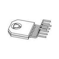
TFA9842J/N1.112 NXP Semiconductors, TFA9842J/N1.112 Datasheet - Page 6

TFA9842J/N1.112
Manufacturer Part Number
TFA9842J/N1.112
Description
Manufacturer
NXP Semiconductors
Datasheet
1.TFA9842JN1.112.pdf
(21 pages)
Specifications of TFA9842J/N1.112
Operational Class
Class-AB
Output Power (typ)
15x1@8Ohm/7.5x2@4OhmW
Audio Amplifier Function
Speaker
Total Harmonic Distortion
0.05@8Ohm@1W%
Single Supply Voltage (typ)
17V
Dual Supply Voltage (typ)
Not RequiredV
Power Supply Requirement
Single
Power Dissipation
35W
Rail/rail I/o Type
No
Single Supply Voltage (min)
9V
Single Supply Voltage (max)
26V
Dual Supply Voltage (min)
Not RequiredV
Dual Supply Voltage (max)
Not RequiredV
Operating Temp Range
-40C to 85C
Operating Temperature Classification
Industrial
Mounting
Through Hole
Pin Count
9
Lead Free Status / RoHS Status
Compliant
Philips Semiconductors
9397 750 12013
Preliminary data
8.4 Supply voltage ripple rejection
8.5 Built-in protection circuits
Standby — The current consumption is very low and the outputs are floating. The
device is in standby mode when V
Mute — The amplifier is DC-biased but not operational (no audio output). This allows
the input coupling capacitors to be charged to avoid pop-noise. The device is in mute
mode when 4.5 V < V
On — The amplifier is operating normally. The operating mode is activated at
V
The supply voltage ripple rejection (SVRR) is measured with an electrolytic capacitor
of 150 F on pin SVR using a bandwidth of 20 Hz to 22 kHz.
SVRR as function of the frequency. A larger capacitor value on pin SVR improves the
ripple rejection behavior at the lower frequencies.
The TFA9842J contains two types of temperature sensors; one measures local
temperatures of the power stages and one measures the global chip temperature. At
a local temperature of the power stage of approximately 185
temperature of approximately 150
stages for 2 ms. High impedance of the outputs is the result. After this time period the
power stages switch on automatically and the detection will take place again; still a
too high temperature switches off the power stages immediately. This protects the
TFA9842J against shorts to ground, to the supply voltage, across the load and too
high chip temperatures.
The protection will only be activated when necessary, so even during a short-circuit
condition, a certain amount of (pulsed) current will still be flowing through the short,
just as much as the power stage can handle without exceeding the critical
temperature level.
Fig 3. Mode selection.
MODE
> (V
CC
standby
2.0 V).
Rev. 01 — 26 April 2004
0.8
MODE
4.5
< (V
CC
MODE
o
C this detection circuit switches off the power
3.5 V).
2-channel audio amplifier (2 x SE or 1 x BTL)
all mute
< 0.8 V, or when pin MODE is grounded.
V CC 3.5
© Koninklijke Philips Electronics N.V. 2004. All rights reserved.
V CC 2.0
1/2 on
Figure 11
o
V MODE (V)
C or a global
TFA9842J
V CC
MCE502
illustrates the
6 of 21


