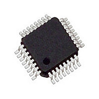
IDTMPC9446FAR2 IDT, Integrated Device Technology Inc, IDTMPC9446FAR2 Datasheet - Page 3

IDTMPC9446FAR2
Manufacturer Part Number
IDTMPC9446FAR2
Description
Manufacturer
IDT, Integrated Device Technology Inc
Type
Clock Dividerr
Datasheet
1.IDTMPC9446FAR2.pdf
(11 pages)
Specifications of IDTMPC9446FAR2
Number Of Clock Inputs
2
Mode Of Operation
Single-Ended
Output Frequency
250MHz
Output Logic Level
LVCMOS
Operating Supply Voltage (min)
2.375V
Operating Supply Voltage (typ)
2.5/3.3V
Operating Supply Voltage (max)
3.465V
Package Type
TQFP
Operating Temp Range
-40C to 85C
Operating Temperature Classification
Industrial
Signal Type
LVCMOS
Mounting
Surface Mount
Pin Count
32
Quiescent Current
2mA
Lead Free Status / RoHS Status
Not Compliant
IDT™ / ICS™ LVCMOS CLOCK FANOUT BUFFER
MPC9446
3.3V AND 2.5V LVCMOS CLOCK FANOUT BUFFER
Table 1. Pin Configuration
Table 2. Supported Single and Dual Supply Configurations
Table 3. Function Table (Controls)
Table 4. Absolute Maximum Ratings
CCLK0,1
FSELA, FSELB, FSELC
MR/OE
GND
V
V
QA0 – QA2
QB0 – QB2
QC0 – QC3
3.3 V
Mixed Voltage Supply
2.5 V
CCLK_SEL
FSELA
FSELB
FSELC
MR/OE
1. V
1. V
2. V
3. V
4. V
1. Absolute maximum continuous ratings are those maximum values beyond which damage to the device may occur. Exposure to these
Symbol
CCA
CC
V
I
V
V
OUT
conditions or conditions beyond those indicated may adversely affect device reliability. Functional operation under absolute-maximum-rated
conditions is not implied.
T
OUT
I
Supply Voltage Configuration
CC
IN
CCB
CC
CCA
CCB
CCC
IN
, V
S
Control
CCB
is the positive power supply of the device core and input circuitry. V
is internally connected to V
is the positive power supply of the bank A outputs. V
is the positive power supply of the bank B outputs. V
is the positive power supply of the bank C outputs. V
Pin
(1)
Supply Voltage
DC Input Voltage
DC Output Voltage
DC Input Current
DC Output Current
Storage Temperature
, V
CCC
Input
Input
Input
Output
Output
Output
Default
Characteristics
0
0
0
0
0
I/O
CC
.
(1)
LVCMOS
LVCMOS
LVCMOS
Supply
Supply
Supply
LVCMOS
LVCMOS
LVCMOS
CCLK0
f
f
f
Outputs enabled
V
QA0:2
QB0:2
QC0:3
3.3 V
3.3 V
2.5 V
CC
(1)
= f
= f
= f
Type
REF
REF
REF
CCA
CCB
CCC
3.3 V or 2.5 V
voltage defines bank A output levels.
voltage defines bank B output levels. V
voltage defines bank C output levels.
V
LVCMOS clock inputs
Output bank divide select input
Internal reset and output (high impedance) control
Negative voltage supply (GND)
Positive voltage supply for output banks
Positive voltage supply for core (VCC)
Bank A outputs
Bank B outputs
Bank C outputs
3.3 V
2.5 V
CCA
0
(2)
CC
voltage defines the input threshold and levels.
–0.3
–0.3
–0.3
Min
–65
V
3.3 V
3.3 V
2.5 V
CCB
(3)
CCLK1
f
f
f
Internal reset outputs disabled (tristate)
QA0:2
QB0:2
QC0:3
Function
V
V
CC
CC
= f
= f
Max
= f
±20
±50
125
3.6
+0.3
+0.3
REF
REF
REF
3.3 V or 2.5 V
CCB
3MPC9446 REV 4 NOVEMBER 28, 2007)
V
÷ 2
÷ 2
÷ 2
3.3 V
2.5 V
CCC
is internally connected to V
(4)
Unit
1
mA
mA
°C
V
V
V
Condition
GND
0 V
0 V
0 V
CC
.


