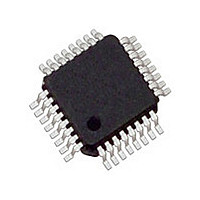
IDTMPC9446FAR2 IDT, Integrated Device Technology Inc, IDTMPC9446FAR2 Datasheet - Page 7

IDTMPC9446FAR2
Manufacturer Part Number
IDTMPC9446FAR2
Description
Manufacturer
IDT, Integrated Device Technology Inc
Type
Clock Dividerr
Datasheet
1.IDTMPC9446FAR2.pdf
(11 pages)
Specifications of IDTMPC9446FAR2
Number Of Clock Inputs
2
Mode Of Operation
Single-Ended
Output Frequency
250MHz
Output Logic Level
LVCMOS
Operating Supply Voltage (min)
2.375V
Operating Supply Voltage (typ)
2.5/3.3V
Operating Supply Voltage (max)
3.465V
Package Type
TQFP
Operating Temp Range
-40C to 85C
Operating Temperature Classification
Industrial
Signal Type
LVCMOS
Mounting
Surface Mount
Pin Count
32
Quiescent Current
2mA
Lead Free Status / RoHS Status
Not Compliant
IDT™ / ICS™ LVCMOS CLOCK FANOUT BUFFER
MPC9446
3.3V AND 2.5V LVCMOS CLOCK FANOUT BUFFER
The time from the PLL controlled edge to the non controlled
edge, divided by the time between PLL controlled edges,
expressed as a percentage.
The pin-to-pin skew is defined as the worst case difference
in propagation delay between any two similar delay paths
within a single device.
t
Figure 7. Output Transition Time Test Reference
F
Figure 9. Output-to-Output Skew t
Figure 11. Output Duty Cycle (DC)
t
P
Figure 6. CCLK0, 1 MPC9446 AC Test Reference for V
Generator
T
Z = 50Ω
0
Pulse
DC = t
t
SK(LH)
t
R
P
/T
0
x 100%
V
CC
0.55
2.4
= 3.3V
t
SK(LH, HL)
SK(HL)
Z
V
V
GND
O
CC
CC
R
V
V
GND
V
V
GND
= 50Ω
V
T
CC
CC
CC
CC
CC
÷2
= 50Ω
1.8V
0.6V
÷2
÷2
= 2.5V
V
TT
MPC9446 DUT
Figure 10. Output Pulse Skew (t
CCLK
Figure 8. Propagation Delay (t
Q
CCLK
X
Qx
CC
Z
t
= 3.3 V and V
(LH)
O
= 50 Ω
t
(LH)
t
SK(P)
R
T
= 50Ω
= | t
CC
PLH
t
(HL)
7MPC9446 REV 4 NOVEMBER 28, 2007)
V
– t
= 2.5 V
TT
t
(HL)
PHL
SK(P)
PD
|
) Test Reference
) Test Reference
V
V
GND
V
V
GND
CC
CC
CC
CC
÷2
÷2
V
V
GND
V
V
GND
CC
CC
CC
CC
÷2
÷2


