NHD-0420DZW-AY5 Newhaven Display, NHD-0420DZW-AY5 Datasheet
NHD-0420DZW-AY5
Specifications of NHD-0420DZW-AY5


Related parts for NHD-0420DZW-AY5


NHD-0420DZW-AY5 Summary of contents
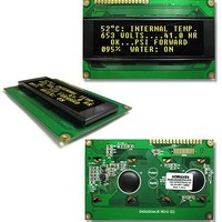
Page 1
... NHD‐0420DZW‐AY5 OLED Display Module NHD‐ Newhaven Display 0420‐ 4 lines x 20 characters DZW‐ OLED A‐ Model Y‐ ...
Page 2
... Parallel or serial MPU interface (Default 6800 MPU parallel) • +3.0V or +5.0V Power Supply • RoHS compliant • Size compatible to NHD‐0420DZ series Character LCDs Description ...
Page 3
... P2.54*15=38.10 2.0 1 16-1.0 PTH 49.0 2.50 0.59 98.0 0.5 94.0 77.0 4-2.5 PTH 4-5 93.0 3.54 2.9 0.54 DOT SIZES SCALE 5/1 10. 4.7 1.60 The non-specified tolerance Newhaven Display NHD-0420DZW-AY5 1 Vss 2 Vdd R DB0 8 DB1 9 DB2 10 DB3 11 DB4 12 DB5 ...
Page 4
Pin Description Parallel Interface (default): Pin No. Symbol External Connection 1 VSS Power Supply 2 VDD Power Supply 3 NC ‐ 4 RS MPU 5 R/W MPU 6 E MPU 7‐10 DB0 – DB3 MPU 11‐14 DB4 – DB7 MPU 15 NC ‐ 16 NC ‐ Serial Interface: Pin No. ...
Page 5
Wiring Diagrams [5] ...
Page 6
Electrical Characteristics Item Operating Temperature Range Storage Temperature Range Supply Voltage Supply Current “H” Level input “L” Level input “H” Level output “L” Level output Optical Characteristics Item Viewing Angle – Vertical (top) Viewing Angle – Vertical (bottom) Viewing Angle – Horizontal (left) Viewing Angle – Horizontal (right) Contrast Ratio Response Time (rise) Response Time (fall) Brightness Lifetime Note: Lifetime at typical temperature is based on accelerated high‐temperature operation. Lifetime is tested at average 50% pixels on and is rated as Hours until Half‐Brightness. The Display OFF command can be used to extend the lifetime of the display. ...
Page 7
Instruction Table Instruction RS R/W DB7 Clear Display 0 0 0 Return 0 0 0 Home Entry Mode 0 0 0 Set Display ON/OFF 0 0 0 control Cursor/Displ 0 0 0 ay Shift Function Set 0 0 0 Set CGRAM 0 0 0 address Set DDRAM ...
Page 8
Clear Display RS R/W DB7 DB6 DB5 0 0 0 0 0 This instruction is used to clear the display by writing 0x20 in all DDRAM addresses. This instruction does not change the DDRAM Address. Return Home RS R/W DB7 DB6 DB5 0 0 0 0 0 This instruction is used to set the DDRAM Address to 0x00 and shifts the display back to the original state. The cursor (if on) will be at the first line’s left‐most character. The DDRAM contents on the display do not change. Entry Mode Set RS R/W DB7 DB6 DB5 0 0 0 0 0 I/D = Increment/Decrement ...
Page 9
Display ON/OFF RS R/W DB7 DB6 DB5 0 0 0 0 0 D = Display ON/OFF When D = “1”, the display is turned ON. When D = “0”, the display is turned OFF. Contents in DDRAM are not changed. C = Cursor ON/OFF When C = “1”, the cursor is displayed. The cursor is displayed as 5 dots on the 8 cursor is OFF. B = Blinking Cursor When B = “1”, the entire character specified by the cursor blinks at a speed of 409.6ms intervals. When B = “0”, the character does not blink, the cursor remains on. Cursor/Display Shift RS R/W DB7 DB6 DB5 0 0 0 0 0 S/C R/L Shift Function 0 ...
Page 10
Set CGRAM Address RS R/W DB7 DB6 DB5 0 0 0 1 ACG5 This instruction is used to set the CGRAM address into the Address Counter. Data can then be written to or read from the CGRAM locations. See section: “How to use CGRAM”. ACG5..ACG0 is the binary CGRAM address. Set DDRAM Address RS R/W DB7 DB6 DB5 0 0 1 ADD6 ADD5 ADD4 ADD3 This instruction is used to set the DDRAM address into the Address Counter. Data can then be written to or read from the DDRAM locations. ADD6..ADD0 is the binary DDRAM address. Line 1 = Address 0x00 through 0x13 Line 2 = Address 0x40 through 0x53 Line 3 = Address 0x14 through 0x27 Line 4 = Address 0x54 through 0x67 1 2 3 ...
Page 11
This instruction is used to read 8‐bits of data to the CGRAM or DDRAM at the current address counter. After the read is complete, the address is automatically incremented or decremented by 1 according to the Entry Mode. The Set CGRAM Address or Set DDRAM Address Instruction must be executed before this instruction can be performed, otherwise the first Read Data will not be valid. MPU Interface When DL is set for 8‐bit mode, the display interfaces with the MPU with DB7..DB0 (DB7 is the MSB). When DL is set for 4‐bit mode, the display interfaces with the MPU with only DB7..DB4 (DB7 is the MSB). Each instruction must be sent in two operations, the 4 high‐order bits first, followed by the 4 low‐order bits. The Busy Flag must be checked after completion of the entire 8‐bit instruction. 6800‐MPU Parallel Interface (default) AS68 CSB 0. DB0 to DB7 DB0 to DB7 Item Signal Address setup time RS Address hold time RS System cycle time Pulse width (write) E Pulse width (read) E ...
Page 12
RS t AS80 CSB RDB, WRB 0.9V DD DB0 to DB7 DB0 to DB7 Item Signal Address setup time RS Address hold time RS System cycle time Pulse width (write) /WR Pulse width (read) /RD Data setup time DB7..DB0 Data hold time DB7..DB0 Read access time DB7..DB0 Output disable time DB7..DB0 ...
Page 13
Serial Interface CSB DB5 0.9V DD (SCL) DB7 (SDI) DB6 (SDO) Item Signal Serial clock cycle DB5 (SCL) SCL high pulse width DB5 (SCL) SCL low pulse width DB5 (SCL) CSB setup time CSB CSB hold time CSB Data setup time DB7 (SDI) Data hold time DB7 (SDI) Read access time DB6 (SDO) ...
Page 14
Built‐in Font Tables English/Japanese (FT[1:0] = 00, default) [14] ...
Page 15
Western European table 1 (FT[1:0] = 01) [15] ...
Page 16
English/Russian (FT[1:0] = 10) [16] ...
Page 17
Western European table 2 (FT[1:0] = 11) [17] ...
Page 18
How to use CGRAM The Character Generator RAM (CGRAM) is used to generate custom 5x8 character patterns. There are 8 available addresses: CGRAM Address 0x00 through 0x08. Character Code DDRAM address on Font Table used to write CGRAM Address CGRAM character to display 5 4 0 0 0x00 0 0 0x01 . . . . 0x02..0x06 . . . . 1 1 1 0x07 Notes: “‐“ = Not used The cursor line position can be used, it will be displayed as a logic‐OR if the cursor is turned ON. CGRAM is stored in positions 0x00 through 0x07 of the font table. Therefore, to write the first CGRAM character to the display, you would move the cursor to the desired DDRAM location on the display and write character data 0x00. ...
Page 19
Initialization Sequence 8‐bit mode: Power ON Wait for power stabilization: ≥ 1ms Function Set: RS R/W DB7 DB6 DB5 0 0 0 0 Check BUSY flag Display OFF: RS R/W DB7 DB6 DB5 0 0 0 0 Check BUSY flag Display Clear: RS R/W DB7 DB6 DB5 0 0 0 0 ...
Page 20
Initialization Sequence 4‐bit mode: Power ON Wait for power stabilization: ≥ 1ms Function Set: RS R/W DB7 DB6 0 0 0 0 0 0 0 0 0 0 1 0 Check BUSY flag Display OFF: RS R/W DB7 DB6 DB5 0 0 0 0 0 0 1 0 Check BUSY flag ...
Page 21
Quality Information Test Item High Temperature storage Test the endurance of the display at high storage temperature. Low Temperature storage Test the endurance of the display at low storage temperature. High Temperature Test the endurance of the display by Operation applying electric stress (voltage & current) at high temperature. Low Temperature Test the endurance of the display by Operation applying electric stress (voltage & current) at low temperature. High Temperature / Test the endurance of the display by Humidity Operation applying electric stress (voltage & current) at high temperature with high humidity. Thermal Shock resistance Test the endurance of the display by applying electric stress (voltage & current) during a cycle of low and high temperatures. Vibration test Test the endurance of the display by applying vibration to simulate transportation and use. Atmospheric Pressure test Test the endurance of the display by applying atmospheric pressure to simulate transportation by air. Static electricity test Test the endurance of the display by ...