NHD-0420DZW-AY5 Newhaven Display, NHD-0420DZW-AY5 Datasheet - Page 10
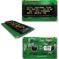
NHD-0420DZW-AY5
Manufacturer Part Number
NHD-0420DZW-AY5
Description
DISPLAY OLED CHAR 4X20 YLW
Manufacturer
Newhaven Display
Datasheet
1.NHD-0420DZW-AY5.pdf
(21 pages)
Specifications of NHD-0420DZW-AY5
Viewing Area (w X H)
77 mm x 25.2 mm
Operating Voltage
5 V
Operating Current
43 mA
Maximum Operating Temperature
+ 80 C
Minimum Operating Temperature
- 40 C
Illumination Color
Yellow
Viewing Angle
80 deg
Lead Free Status / Rohs Status
Lead free / RoHS Compliant


Set CGRAM Address
This instruction is used to set the CGRAM address into the Address Counter. Data can then be written to or read from
the CGRAM locations. See section: “How to use CGRAM”.
ACG5..ACG0 is the binary CGRAM address.
Set DDRAM Address
This instruction is used to set the DDRAM address into the Address Counter. Data can then be written to or read from
the DDRAM locations.
ADD6..ADD0 is the binary DDRAM address.
Line 1 = Address 0x00 through 0x13
Line 2 = Address 0x40 through 0x53
Line 3 = Address 0x14 through 0x27
Line 4 = Address 0x54 through 0x67
Read Busy Flag and Address Counter
This instruction is used to read the Busy Flag (BF) to indicate if the display controller is performing an internal operation.
The Address Counter is read simultaneously with checking the Busy Flag.
When BF = “1”, the controller is busy and the next instruction will be ignored.
When BF = “0”, the controller is not busy and is ready to accept instructions.
AC6..AC0 is the binary location of either the CGRAM or DDRAM current address.
Write Data to CGRAM or DDRAM
This instruction is used to write 8‐bits of data to the CGRAM or DDRAM at the current address counter. After the write is
complete, the address is automatically incremented or decremented by 1 according to the Entry Mode.
Read Data from CGRAM or DDRAM
RS
RS
RS
RS
RS
0
0
0
1
1
R/W
R/W
R/W
R/W
R/W
0
0
1
0
1
1
00
40
14
54
2
01
41
15
55
DB7
DB7
DB7
DB7
DB7
BF
0
1
3
02
42
16
56
ADD6 ADD5 ADD4 ADD3
DB6
DB6
DB6
AC6
DB6
DB6
1
4
03
43
17
57
5
04
44
18
58
ACG5
DB5
DB5
DB5
DB5
DB5
AC5
6
05
45
19
59
ACG4
DB4
DB4
DB4
DB4
DB4
AC4
7
06
46
1A
5A
Write Data
Read Data
8
07
47
1B
5B
ACG3
DB3
DB3
DB3
AC3
DB3
DB3
9
08
48
1C
5C
ADD2
ACG2
10
09
49
1D
5D
DB2
DB2
DB2
AC2
DB2
DB2
[10]
11
0A
4A
1E
5E
ACG1
ADD1
DB1
DB1
DB1
DB1
DB1
AC1
12
0B
4B
1F
5F
ADD0
ACG0
DB0
DB0
13
0C
4C
20
60
DB0
DB0
DB0
AC0
14
0D
4D
21
61
15
0E
4E
22
62
16
0F
4F
23
63
17
10
50
24
64
18
11
51
25
65
19
12
52
26
66
20
13
53
27
67
Related parts for NHD-0420DZW-AY5
Image
Part Number
Description
Manufacturer
Datasheet
Request
R

Part Number:
Description:
LCD COG GRAPH 128X64 NO REFL
Manufacturer:
Newhaven Display
Part Number:
Description:
LCD COG GRAPH 128X64 NO REFL
Manufacturer:
Newhaven Display
Part Number:
Description:
LCD COG GRAPH 128X64 WH TRANSFL
Manufacturer:
Newhaven Display
Part Number:
Description:
LCD COG GRAPH 128X64 WH TRANSFL
Manufacturer:
Newhaven Display

Part Number:
Description:
DISPLAY VFD ALPHA 1X20 6.5MM
Manufacturer:
Newhaven Display
Datasheet:

Part Number:
Description:
DISPLAY VFD ALPHA 1X16 5MM
Manufacturer:
Newhaven Display
Datasheet:

Part Number:
Description:
DISPLAY VFD 7-SEG 1X9 9.7MM
Manufacturer:
Newhaven Display
Datasheet:

Part Number:
Description:
DISPLAY VFD 7-SEG 1X6 20MM
Manufacturer:
Newhaven Display
Datasheet:

Part Number:
Description:
DISPLAY VFD 7-SEG 1X19 11MM
Manufacturer:
Newhaven Display
Datasheet:

Part Number:
Description:
DISPLAY VFD 7-SEG 1X3 8MM
Manufacturer:
Newhaven Display
Datasheet:

Part Number:
Description:
DISPLAY VFD CUSTOM DVD
Manufacturer:
Newhaven Display
Datasheet:

Part Number:
Description:
DISPLAY VFD CUST AUDIO
Manufacturer:
Newhaven Display
Datasheet:

Part Number:
Description:
DISPLAY VFD CUST AUDIO
Manufacturer:
Newhaven Display
Datasheet:

Part Number:
Description:
DISPLAY VFD 7-SEG 1X5 7.6MM
Manufacturer:
Newhaven Display
Datasheet:

Part Number:
Description:
DISPLAY VFD CUST APPLIANCE
Manufacturer:
Newhaven Display
Datasheet: