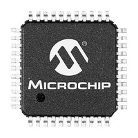
PIC24FV32KA304-I/PT Microchip Technology, PIC24FV32KA304-I/PT Datasheet - Page 148

PIC24FV32KA304-I/PT
Manufacturer Part Number
PIC24FV32KA304-I/PT
Description
MCU 32KB FLASH 2KB RAM 44-TQFP
Manufacturer
Microchip Technology
Specifications of PIC24FV32KA304-I/PT
Processor Series
PIC24FV
Core
PIC
Data Bus Width
16 bit
Program Memory Type
Flash
Program Memory Size
32 KB
Data Ram Size
2 KB
Maximum Operating Temperature
+ 85 C
Mounting Style
SMD/SMT
Package / Case
TQFP-44
Development Tools By Supplier
MPLAB IDE Software
Minimum Operating Temperature
- 40 C
Lead Free Status / Rohs Status
Lead free / RoHS Compliant
Available stocks
Company
Part Number
Manufacturer
Quantity
Price
Company:
Part Number:
PIC24FV32KA304-I/PT
Manufacturer:
VISHAY
Quantity:
12 000
Company:
Part Number:
PIC24FV32KA304-I/PT
Manufacturer:
Microchip Technology
Quantity:
10 000
- Current page: 148 of 320
- Download datasheet (3Mb)
PIC24FV32KA304 FAMILY
REGISTER 13-1:
DS39995B-page 148
bit 15
bit 7
Legend:
R = Readable bit
-n = Value at POR
bit 15
bit 14
bit 13
bit 12-7
bit 6
bit 5-4
bit 3
bit 2
bit 1
bit 0
Note 1:
R/W-0
TON
U-0
—
In 32-bit mode, the T3CON or T5CON control bits do not affect 32-bit timer operation.
TON: Timer2 On bit
When TxCON<3> = 1:
1 = Starts 32-bit Timerx/y
0 = Stops 32-bit Timerx/y
When TxCON<3> = 0:
1 = Starts 16-bit Timerx
0 = Stops 16-bit Timerx
Unimplemented: Read as ‘0’
TSIDL: Stop in Idle Mode bit
1 = Discontinue module operation when device enters Idle mode
0 = Continue module operation in Idle mode
Unimplemented: Read as ‘0’
TGATE: Timerx Gated Time Accumulation Enable bit
When TCS = 1:
This bit is ignored.
When TCS = 0:
1 = Gated time accumulation is enabled
0 = Gated time accumulation is disabled
TCKPS<1:0>: Timerx Input Clock Prescale Select bits
11 = 1:256
10 = 1:64
01 = 1:8
00 = 1:1
T32: 32-Bit Timer Mode Select bit
1 = Timer2 and Timer3 or Timer4 and Timer5 form a single 32-bit timer
0 = Timer2 and Timer3 or Timer4 and Timer5 act as two 16-bit timers
Unimplemented: Read as ‘0’
TCS: Timerx Clock Source Select bit
1 = External clock from pin, TxCK (on the rising edge)
0 = Internal clock (F
Unimplemented: Read as ‘0’
TGATE
R/W-0
U-0
—
TxCON: TIMER2 AND TIMER4 CONTROL REGISTER
W = Writable bit
‘1’ = Bit is set
TCKPS1
R/W-0
TSIDL
R/W-0
OSC
/2)
TCKPS0
R/W-0
(1)
U-0
—
U = Unimplemented bit, read as ‘0’
‘0’ = Bit is cleared
R/W-0
T32
U-0
—
(1)
U-0
U-0
—
—
2011 Microchip Technology Inc.
x = Bit is unknown
R/W-0
TCS
U-0
—
U-0
U-0
—
—
bit 8
bit 0
Related parts for PIC24FV32KA304-I/PT
Image
Part Number
Description
Manufacturer
Datasheet
Request
R

Part Number:
Description:
Manufacturer:
Microchip Technology Inc.
Datasheet:

Part Number:
Description:
Manufacturer:
Microchip Technology Inc.
Datasheet:

Part Number:
Description:
Manufacturer:
Microchip Technology Inc.
Datasheet:

Part Number:
Description:
Manufacturer:
Microchip Technology Inc.
Datasheet:

Part Number:
Description:
Manufacturer:
Microchip Technology Inc.
Datasheet:

Part Number:
Description:
Manufacturer:
Microchip Technology Inc.
Datasheet:

Part Number:
Description:
Manufacturer:
Microchip Technology Inc.
Datasheet:

Part Number:
Description:
Manufacturer:
Microchip Technology Inc.
Datasheet:


