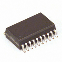
MC88LV926DWR2 Freescale Semiconductor, MC88LV926DWR2 Datasheet - Page 8

MC88LV926DWR2
Manufacturer Part Number
MC88LV926DWR2
Description
IC DRIVER CLK PLL 66MHZ 20-SOIC
Manufacturer
Freescale Semiconductor
Type
PLL Clock Driverr
Datasheet
1.MC88LV926DWR2.pdf
(12 pages)
Specifications of MC88LV926DWR2
Input
CMOS, TTL
Output
CMOS
Frequency - Max
66MHz
Voltage - Supply
3 V ~ 3.6 V
Operating Temperature
0°C ~ 70°C
Mounting Type
Surface Mount
Package / Case
20-SOIC (7.5mm Width)
Frequency-max
66MHz
Lead Free Status / RoHS Status
Contains lead / RoHS non-compliant
Other names
MC88LV926DWR2TR
Available stocks
Company
Part Number
Manufacturer
Quantity
Price
MC88LV926
1. Figure 6. shows a loop filter and analog isolation scheme
1a. All loop filter and analog isolation components should be
1b. The 47
MOTOROLA
The t PD spec includes the full temperature range from 0 C
to 70 C and the full V CC range from 3.0V to 3.3V. If the T
and V CC is a given system are less than the specification
limits, the t PD spec window will be reduced. The t PD
window for a given T and V CC is given by the following
regression formula:
which will be effective in most applications. The following
guidelines should be followed to ensure stable and
jitter–free operation:
tied as close to the package as possible. Stray current
passing through the parasitics of long traces can cause
undesirable voltage transients at the RC1 pin.
capacitor, and the 0.1 F high frequency bypass capacitor
form a wide bandwidth filter that will make the 88LV926
PLL insensitive to voltage transients from the system
digital V CC supply and ground planes. This filter will
typically ensure that a 100mV step deviation on the digital
V CC supply will cause no more than a 100ps phase
deviation on the 88LV926 outputs. A 250mV step
deviation on V CC using the recommended filter values
will cause no more than a 250ps phase deviation; if a
25 F bypass capacitor is used (instead of 10 F) a
250mV V CC step will cause no more than a 100ps phase
deviation.
If good bypass techniques are used on a board design
near components which may cause digital V CC and
ground noise, the above described V CC step deviations
should not occur at the 88LV926’s digital V CC supply. The
NOTE: FURTHER LOOP OPTIMIZATION MAY OCCUR
resistors, the 10 F low frequency bypass
Figure 6. Recommended Loop Filter and Analog Isolation Scheme for the MC88LV926
10 F LOW
FREQ BIAS
TBD
Notes Concerning Loop Filter and Board Layout Issues
0.1 F HIGH
FREQ BIAS
470K
47
47
BOARD GND
BOARD V CC
8
0.1 F (LOOP
FILTER CAP)
330
5. The RST_OUT pin is an open drain N–Channel output.
1c. There are no special requirements set forth for the loop
1d. The 470K reference resistor injects current into the
2. In addition to the bypass capacitors used in the analog
Therefore an external pull–up resistor must be provide to
pull up the RST_OUT pin when it goes into the high
impedance state (after the MC88LV926 is phase–locked
to the reference input with RST_IN held high or 1024 ‘Q’
cycles after the RST_IN pin goes high when the part is
locked). In the t PLZ and t PZL specifications, a 1K resistor
is used as a pull–up as shown in Figure 3.
A SEPARATE ANALOG POWER SUPPLY IS NOT NECESSARY AND
SHOULD NOT BE USED. FOLLOWING THESE PRESCRIBED GUIDE-
LINES IS ALL THAT IS NECESSARY TO USE THE MC88LV926 IN A NOR-
MAL DIGITAL ENVIRONMENT.
purpose of the bypass filtering scheme shown in Figure
6. is to give the 88LV926 additional protection from the
power supply and ground plane transients that can occur
in a high frequency, high speed digital system.
filter resistors (470K and 330 ). The loop filter capacitor
(0.1uF) can be a ceramic chip capacitor, the same as a
standard bypass capacitor.
internal charge pump of the PLL, causing a fixed offset
between the outputs and the SYNC input. This also
prevents excessive jitter caused by inherent PLL
dead–band. If the VCO (2X_Q output) is running above
40MHz, the 470K resistor provides the correct amount of
current injection into the charge pump (2–3 A). If the
VCO is running below 40MHz, a 1M
should be used (instead of 470K).
filter of Figure 6., there should be a 0.1 F bypass
capacitor between each of the other (digital) four V CC
pins and the board ground plane. This will reduce output
switching noise caused by the 88LV926 outputs, in
addition to reducing potential for noise in the ‘analog’
section of the chip. These bypass capacitors should also
be tied as close to the 88LV926 package as possible.
5
6
7
ANALOG V CC
RC1
ANALOG GND
ANALOG LOOP FILTER/VCO
SECTION OF THE MC88LV926
20–PIN SOIC PACKAGE (NOT
DRAWN TO SCALE)
TIMING SOLUTIONS
reference resistor


