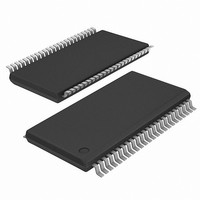
ICS952302AGT IDT, Integrated Device Technology Inc, ICS952302AGT Datasheet

ICS952302AGT
Specifications of ICS952302AGT
Related parts for ICS952302AGT
ICS952302AGT Summary of contents
Page 1
Integrated Circuit Systems, Inc. Frequency Generator for Transmeta Recommended Application: Transmeta Efficion, ATi M6 Output Features: • CPUs @ 3.3V including 1 free running CPUCLK_F • PCI @ 3.3V, including 4 free running PCICLK_F • 1 ...
Page 2
ICS952302 Pin Descriptions PIN PIN # PIN NAME TYPE 1 VDDREF PWR 2 REF0 OUT 3 GNDREF PWR OUT 6 VDDPCI PWR 7 PCICLK_F0 OUT 8 PCICLK_F1 OUT 9 GNDPCI PWR 10 PCICLK0 OUT 11 ...
Page 3
General Description Spread spectrum may be enabled through SMBus programming. Spread spectrum typically reduces system EMI by 8dB to 10dB. This simplifies EMI qualification without resorting to board design iterations or costly shielding. The ICS952302 employs a proprietary closed loop ...
Page 4
ICS952302 SMBus Table: Output Control Register Byte 0 Pin # Name 42 Bit 7 CPUCLK_F 45 Bit 6 CPUCLK0 43 Bit 5 CPUCLK1 32 Bit 4 27MHZ 25 Bit 3 48MHZ_0 26 Bit 2 48MHZ_1 2 Bit 1 REF0 48 ...
Page 5
SMBus Table: Spread Spectrum Control Register Byte 4 Pin # Name Bit 7 - Spread Position - Bit 6 SS1 - Bit 5 SS2 - Bit 4 Bit Bit 2 Bit Bit 0 SMBus ...
Page 6
ICS952302 Absolute Maximum Ratings Supply Voltage . . . . . . . . . . . . . . . . . . . . . . . 5.5 V Logic Inputs . . . . . . . ...
Page 7
Electrical Characteristics - CPU 70° 3.3 V +/-5 PARAMETER SYMBOL V Output High Voltage OH2B Output Low Voltage V OL2B I Output High Current OH2B I Output Low Current OL2B 1 ...
Page 8
ICS952302 Electrical Characteristics - 27MHz 70° 3.3 V +/-5 PARAMETER SYMBOL Frequency Accuracy F ACC Output High Voltage V OH2B V Output Low Voltage OL2B I Output High Current OH2B I ...
Page 9
Electrical Characteristics - REF 70° 3.3 V +/-5 PARAMETER SYMBOL Frequency Accuracy F ACC Output High Voltage V OH2B V Output Low Voltage OL2B I Output High Current OH2B I Output ...
Page 10
ICS952302 General SMBus serial interface information for the ICS952302 How to Write: • Controller (host) sends a start bit. • Controller (host) sends the write address D2 • ICS clock will acknowledge • Controller (host) sends the begining byte location ...
Page 11
Shared Pin Operation - Input/Output Pins The I/O pins designated by (input/output) serve as dual signal functions to the device. During initial power-up, they act as input pins. The logic level (voltage) that is present on these pins at this ...
Page 12
ICS952302 PD# Timing Diagram The power down selection is used to put the part into a very low power state without turning off the power to the part. PD asynchronous active low input. This signal needs to be ...
Page 13
CLK_STOP# Timing Diagram CLK_STOP asychronous input to the clock synthesizer used to turn off the CPU clocks for low power operation. CLK_STOP# is synchronized by the ICS952302. The minimum that the CPU clock is enabled (CLK_STOP# ...
Page 14
ICS952302 PCI_STOP# Timing Diagram PCI_STOP asynchronous input to the ICS952302 used to turn off the PCICLK clocks for low power operation. PCI_STOP# is synchronized by the ICS952302 internally. The minimum that the PCICLK clocks are enabled ...
Page 15
INDEX INDEX AREA AREA aaa (0.020 mil) (240 mil) 6.10 mm. Body, 0.50 mm. pitch TSSOP Ordering Information ICS952302yGLF-T Example: ICS XXXX y G LF- T 0957B—10/05/04 ...


