ICS9DB823BGLFT IDT, Integrated Device Technology Inc, ICS9DB823BGLFT Datasheet - Page 5
ICS9DB823BGLFT
Manufacturer Part Number
ICS9DB823BGLFT
Description
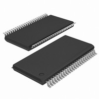
IC PC CLOCK 3.3V 48-TSSOP
Manufacturer
IDT, Integrated Device Technology Inc
Type
Clock Bufferr
Datasheet
1.ICS9DB823BGLFT.pdf
(21 pages)
Specifications of ICS9DB823BGLFT
Input
Clock
Output
Clock
Frequency - Max
400MHz
Voltage - Supply
3.135 V ~ 3.465 V
Operating Temperature
0°C ~ 70°C
Mounting Type
Surface Mount
Package / Case
48-TSSOP
Frequency-max
400MHz
Lead Free Status / RoHS Status
Lead free / RoHS Compliant
Other names
9DB823BGLFT


Pin Description for OE_INV = 1
IDT
PIN #
9DB823B
Eight Output Differential Buffer for PCIe for Gen 1, Gen 2 and QPI
10
11
12
13
14
15
16
17
18
19
20
21
22
23
24
®
1
2
3
4
5
6
7
8
9
Eight Output Differential Buffer for PCIe Gen 1, Gen 2 and QPI
SRC_DIV#
VDD
GND
SRC_IN
SRC_IN#
OE0#
OE3#
DIF_0
DIF_0#
GND
VDD
DIF_1
DIF_1#
OE1#
OE2#
DIF_2
DIF_2#
GND
VDD
DIF_3
DIF_3#
BYPASS#_133_100
SCLK
SDATA
PIN NAME
PIN TYPE
PWR
PWR
PWR
PWR
PWR
PWR
OUT
OUT
OUT
OUT
OUT
OUT
OUT
OUT
I/O
IN
IN
IN
IN
IN
IN
IN
IN
IN
Active low Input for determining SRC output frequency SRC or SRC/2.
0 = SRC/2, 1= SRC
Power supply, nominal 3.3V
Ground pin.
0.7 V Differential SRC TRUE input
0.7 V Differential SRC COMPLEMENTARY input
Active low input for enabling DIF pair 0.
1 =disable outputs, 0 = enable outputs
Active low input for enabling DIF pair 3.
1 =disable outputs, 0 = enable outputs
0.7V differential true clock output
0.7V differential Complementary clock output
Ground pin.
Power supply, nominal 3.3V
0.7V differential true clock output
0.7V differential Complementary clock output
Active low input for enabling DIF pair 1.
1 =disable outputs, 0 = enable outputs
Active low input for enabling DIF pair 2.
1 =disable outputs, 0 = enable outputs
0.7V differential true clock output
0.7V differential Complementary clock output
Ground pin.
Power supply, nominal 3.3V
0.7V differential true clock output
0.7V differential Complementary clock output
Input to select Bypass(fan-out), QPI PLL (133MHz) or PCIe PLL (100MHz) mode
0 = Bypass mode, M= QPI, 1= PCIe PLL mode
Clock pin of SMBus circuitry, 5V tolerant.
Data pin for SMBus circuitry, 5V tolerant.
5
DESCRIPTION
1444D - 08/31/10
Related parts for ICS9DB823BGLFT
Image
Part Number
Description
Manufacturer
Datasheet
Request
R

Part Number:
Description:
TRANSLATION DEVICE DPI 80-PQFP
Manufacturer:
IDT, Integrated Device Technology Inc
Datasheet:
Part Number:
Description:
IDT PART
Manufacturer:
IDT, Integrated Device Technology Inc
Datasheet:
Part Number:
Description:
IC LIU T1/E1/J1 OCTAL 256PBGA
Manufacturer:
IDT, Integrated Device Technology Inc
Datasheet:

Part Number:
Description:
IC FREQ TIMING GENERATOR 28TSSOP
Manufacturer:
IDT, Integrated Device Technology Inc
Datasheet:
Part Number:
Description:
IC CLK DVR PLL 1:10 40VFQFPN
Manufacturer:
IDT, Integrated Device Technology Inc
Datasheet:
Part Number:
Description:
IC CLK FANOUT BUFFER 1:18 32LQFP
Manufacturer:
IDT, Integrated Device Technology Inc
Datasheet:
Part Number:
Description:
IC CLK FANOUT BUFFER 1:18 32LQFP
Manufacturer:
IDT, Integrated Device Technology Inc
Datasheet:
Part Number:
Description:
IC CK505 VREG/RES 56TSSOP
Manufacturer:
IDT, Integrated Device Technology Inc
Datasheet:

Part Number:
Description:
IC SDRAM CLK DVR 1:10 48-TSSOP
Manufacturer:
IDT, Integrated Device Technology Inc
Datasheet:

Part Number:
Description:
IC CLK DVR PLL 1:10 48TSSOP
Manufacturer:
IDT, Integrated Device Technology Inc
Datasheet:
Part Number:
Description:
IC FLEXPC CLK PROGR P4 56-TSSOP
Manufacturer:
IDT, Integrated Device Technology Inc
Datasheet:
Part Number:
Description:
IC FLEXPC CLK PROGR P4 56-TSSOP
Manufacturer:
IDT, Integrated Device Technology Inc
Datasheet:
Part Number:
Description:
IC FLEXPC CLK PROGR P4 56-SSOP
Manufacturer:
IDT, Integrated Device Technology Inc
Datasheet:

Part Number:
Description:
IC PLL CLK DRIVER 2.5V 28-TSSOP
Manufacturer:
IDT, Integrated Device Technology Inc
Datasheet:
Part Number:
Description:
IC CLOCK DRIVER 2.5V 24-TSSOP
Manufacturer:
IDT, Integrated Device Technology Inc
Datasheet: