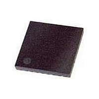
SI5319C-C-GM Silicon Laboratories Inc, SI5319C-C-GM Datasheet - Page 41

SI5319C-C-GM
Manufacturer Part Number
SI5319C-C-GM
Description
IC CLOCK MULT/ATTENUATOR 36QFN
Manufacturer
Silicon Laboratories Inc
Datasheet
1.SI5319C-C-GMR.pdf
(50 pages)
Specifications of SI5319C-C-GM
Input
*
Output
*
Frequency - Max
*
Voltage - Supply
*
Operating Temperature
*
Mounting Type
Surface Mount
Package / Case
36-VFQFN Exposed Pad
Frequency-max
*
Lead Free Status / RoHS Status
Lead free / RoHS Compliant
Available stocks
Company
Part Number
Manufacturer
Quantity
Price
Company:
Part Number:
SI5319C-C-GM
Manufacturer:
Mini
Quantity:
5 000
Part Number:
SI5319C-C-GM
Manufacturer:
SILICON LABS/èٹ¯ç§‘
Quantity:
20 000
Note: Internal register names are indicated by underlined italics (e.g., INT_PIN. See Si5319 Register Map).
19,20
Pin #
8, 31
15
16
17
18
21
22
23
11
7
6
SDA_SDO
Pin Name
RATE0
RATE1
CKIN+
CKIN–
GND
LOL
SCL
CS
XB
XA
GND
I/O
I/O
O
I
I
I
I
I
Signal Level
LVCMOS
LVCMOS
LVCMOS
LVCMOS
3-Level
Analog
Supply
Multi
External Crystal or Reference Clock.
External crystal should be connected to these pins to use internal
oscillator based reference. Refer to the Family Reference Manual for
interfacing to an external reference. The external reference must be
from a high-quality clock source (TCXO, OCXO). Frequency of crystal
or external clock is set by the RATE pins.
Ground.
Must be connected to system ground. Minimize the ground path
impedance for optimal performance of this device. Grounding these
pins does not eliminate the requirement to ground the GND PAD on
the bottom of the package.
External Crystal or Reference Clock Rate.
Three level inputs that select the type and rate of external crystal or
reference clock to be applied to the XA/XB port. Refer to the Family
Reference Manual for settings. These pins have both a weak pull-up
and a weak pull-down; they default to M. The "HH" setting is not sup-
ported.
Note: L setting corresponds to ground.
Some designs may require an external resistor voltage divider when
driven by an active device that will tri-state.
Clock Input.
Differential input clock. This input can also be driven with a single-
ended signal. Input frequency range is 2 kHz to 710 MHz.
PLL Loss of Lock Indicator.
This pin functions as the active high PLL loss of lock indicator if the
LOL_PIN register bit is set to 1.
0 = PLL locked.
1 = PLL unlocked.
If LOL_PIN = 0, this pin will tristate. Active polarity is controlled by the
LOL_POL bit. The PLL lock status will always be reflected in the
LOL_INT read only register bit.
Xtal/Input Clock Select.
This pin selects the active DSPLL input clock, which can be a clock
input or a crystal input. See the FREE_EN register for free run settings.
0 = Select clock input (CKIN).
1 = Select crystal or external reference clock.
This pin should not be left open.
Serial Clock/Serial Clock.
This pin functions as the serial clock input for both SPI and I
This pin has a weak pull-down.
Serial Data.
In I
tional serial data port.
In SPI control mode (CMODE = 1), this pin functions as the serial data
output.
2
C control mode (CMODE = 0), this pin functions as the bidirec-
M setting corresponds to V
H setting corresponds to V
Rev. 1.0
Description
DD
DD
.
/2.
Si5319
2
C modes.
41


