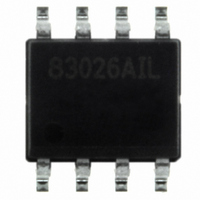
ICS83026AMILF IDT, Integrated Device Technology Inc, ICS83026AMILF Datasheet - Page 4

ICS83026AMILF
Manufacturer Part Number
ICS83026AMILF
Description
IC FANOUT BUFFER 1:2 DIFF 8-SOIC
Manufacturer
IDT, Integrated Device Technology Inc
Series
HiPerClockS™r
Type
Fanout Buffer (Distribution)r
Datasheet
1.ICS83026AMILF.pdf
(12 pages)
Specifications of ICS83026AMILF
Number Of Circuits
1
Ratio - Input:output
1:2
Differential - Input:output
Yes/No
Input
HCSL, LVDS, LVHSTL, LVPECL, SSTL
Output
LVCMOS, LVTTL
Frequency - Max
350MHz
Voltage - Supply
3 V ~ 3.6 V
Operating Temperature
-40°C ~ 85°C
Mounting Type
Surface Mount
Package / Case
8-SOIC
Frequency-max
350MHz
Number Of Outputs
2
Operating Supply Voltage (max)
3.6V
Operating Temp Range
-40C to 85C
Propagation Delay Time
2.5ns
Operating Supply Voltage (min)
3V
Mounting
Surface Mount
Pin Count
8
Operating Supply Voltage (typ)
3.3V
Package Type
SOIC N
Duty Cycle
60%
Operating Temperature Classification
Industrial
Lead Free Status / RoHS Status
Lead free / RoHS Compliant
Other names
800-1103
800-1103-5
800-1103
83026AMILF
800-1103-5
800-1103
83026AMILF
Available stocks
Company
Part Number
Manufacturer
Quantity
Price
Company:
Part Number:
ICS83026AMILFT
Manufacturer:
REALTEK
Quantity:
2 300
Company:
Part Number:
ICS83026AMILFT
Manufacturer:
IDT
Quantity:
3
Part Number:
ICS83026AMILFT
Manufacturer:
IDT
Quantity:
20 000
ICS83026I Data Sheet
AC Electrical Characteristics
Table 4. AC Characteristics, V
NOTE: Electrical parameters are guaranteed over the specified ambient operating temperature range, which is established when the device is
mounted in a test socket with maintained transverse airflow greater than 500 lfpm. The device will meet specifications after thermal equilibrium
has been reached under these conditions.
All parameters measured at f
NOTE 1: Measured from the differential input crossing point to the output at V
NOTE 2: Defined as skew between outputs at the same supply voltage and with equal load conditions. Measured at V
NOTE 3: Defined as skew between outputs on different devices operating at the same supply voltage and with equal load conditions. Using
the same type of inputs on each device, the outputs are measured at V
NOTE 4: This parameter is defined in accordance with JEDEC Standard 65.
ICS83026AMI REVISION C AUGUST 26, 2009
Symbol
f
t
tsk(o)
tsk(pp)
tjit
t
odc
MAX
PD
R
/ t
F
Parameter
Output Skew; NOTE 2, 4
Output Duty Cycle
Output Frequency
Propagation Delay, NOTE 1
Part-to-Part Skew; NOTE 3, 4
Buffer Additive Phase Jitter, RMS;
refer to Additive Phase Jitter Section
Output Rise/Fall Time
MAX
unless noted otherwise.
DD
= 3.3V ± 0.3V, T
125MHz, Integration Range
A
= -40°C to 85°C
(12kHz – 20MHz)
Test Conditions
ƒ ≤ 350MHz
0.8V to 2V
4
DD
/2.
LOW SKEW, 1-TO-2, DIFFERENTIAL-TO-LVCMOS/LVTTL FANOUT BUFFER
DD
/2.
Minimum
150
1.7
40
Typical
©2009 Integrated Device Technology, Inc.
0.092
350
300
2.1
50
5
Maximum
DD
/2.
600
450
2.5
20
60
Units
MHz
ns
ps
ps
ps
ps
%


