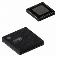
PCK210BS,118 NXP Semiconductors, PCK210BS,118 Datasheet - Page 2

PCK210BS,118
Manufacturer Part Number
PCK210BS,118
Description
IC DRVR CLK ECL/PECL 1:5 32HUQFN
Manufacturer
NXP Semiconductors
Type
Fanout Buffer (Distribution)r
Datasheet
1.PCK210BS118.pdf
(10 pages)
Specifications of PCK210BS,118
Number Of Circuits
2
Ratio - Input:output
1:5
Differential - Input:output
Yes/Yes
Input
ECL, PECL
Output
PECL
Frequency - Max
1.5GHz
Voltage - Supply
2.25 V ~ 3.8 V
Operating Temperature
-40°C ~ 85°C
Mounting Type
Surface Mount
Package / Case
32-VQFN Exposed Pad, 32-HVQFN, 32-SQFN, 32-DHVQFN
Frequency-max
1.5GHz
Lead Free Status / RoHS Status
Lead free / RoHS Compliant
Other names
568-2032-2
935276302118
PCK210BS-T
935276302118
PCK210BS-T
pairs will be used, and therefore terminated. In the case where fewer
Philips Semiconductors
FEATURES
DESCRIPTION
The PCK210 is a low skew 1-to-5 dual differential driver, designed
with clock distribution in mind. The input signals can be either
differential or single-ended if the V
fanned out to 5 identical differential outputs.
The PCK210 is specifically designed, modeled and produced with
low skew as the key goal. Optimal design and layout serve to
minimize gate-to-gate skew within a device, and empirical modeling
is used to determine process control limits that ensure consistent
t
guaranteed low skew device.
To ensure that the tight skew specification is met, it is necessary that
both sides of the differential output are terminated into 50 , even if
only one side is being used. In most applications, all ten differential
than ten pairs are used, it is necessary to terminate at least the
output pairs on the same package side as the pair(s) being used on
that side, in order to maintain minimum skew. Failure to do this will
result in small degradations of propagation delay (on the order of
10–20 ps) of the output(s) being used, which, while not being
catastrophic to most designs, will mean a loss of skew margin.
The PCK210, as with most other ECL devices, can be operated
from a positive V
to be used for high performance clock distribution in +3.3 V or
+2.5 V systems. Designers can take advantage of the PCK210’s
performance to distribute low skew clocks across the backplane or
the board. In a PECL environment, series or Thevenin line
terminations are typically used as they require no additional power
supplies.
The PCK210 may be driven single-endedly utilizing the V
output with the CLKA or CLKB input. If a single-ended signal is to be
used, the V
and bypassed to ground via a 0.01 F capacitor. The V
can only source/sink 0.3 mA, therefore, it should be used as a
switching reference for the PCK210 only. Part-to-part skew
specifications are not guaranteed when driving the PCK210
single-endedly.
ORDERING INFORMATION
PD
Type n mber
Type number
PCK210BD
PCK210BS
2004 Apr 23
85 ps part-to-part skew typical
20 ps output-to-output skew typical
Differential design
V
Voltage and temperature compensated outputs
Low voltage V
75 k input pull-down resistors
Form, fit, and function compatible with MC100EP210
Low voltage dual 1:5 differential
ECL/PECL clock driver
BB
distributions from lot to lot. The net result is a dependable,
output
BB
pin should be connected to the CLKA or CLKB input
EE
CC
Package
Name
LQFP32
HVQFN32
range of –2.25 V to –3.8 V
supply in PECL mode. This allows the PCK210
Description
plastic low profile quad flat package; 32 leads; body 7
plastic thermal enhanced very thin quad flat package; no leads;
32 terminals; body 5
BB
output is used. The signal is
5
BB
BB
output
0.85 mm
bias
2
PINNING
Pin configurations
CLKA
CLKA
CLKB
CLKB
V
n.c.
V
V
CC
BB
EE
CLKA
CLKA
CLKB
CLKB
V
V
V
n.c.
CC
7
1
2
3
4
5
6
7
8
BB
EE
Figure 2. HVQFN32 pin configuration
Figure 1. LQFP32 pin configuration
1.4 mm
1
2
3
4
5
6
7
8
PCK210BD
PCK210BS
(TOP VIEW)
Version
SOT358-1
SOT617-1
Temperature
range
–40 C to +85 C
–40 C to +85 C
PCK210
24
23
22
21
20
19
18
17
p
24
23
22
21
20
19
18
17
Product data
SW02237
QA3
QA3
QA4
QA4
QB0
QB0
QB1
QB1
SW00909
QA3
QA3
QA4
QA4
QB0
QB0
QB1
QB1


