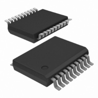
PCK3807ADB,118 NXP Semiconductors, PCK3807ADB,118 Datasheet - Page 2

PCK3807ADB,118
Manufacturer Part Number
PCK3807ADB,118
Description
IC CLOCK DISTRIB LVTTL 20SSOP
Manufacturer
NXP Semiconductors
Type
Fanout Buffer (Distribution)r
Datasheet
1.PCK3807APW118.pdf
(13 pages)
Specifications of PCK3807ADB,118
Package / Case
20-SSOP
Number Of Circuits
1
Ratio - Input:output
1:10
Differential - Input:output
No/No
Input
LVCMOS, LVTTL
Output
LVTTL
Frequency - Max
400MHz
Voltage - Supply
2.3 V ~ 3.6 V
Operating Temperature
-40°C ~ 85°C
Mounting Type
Surface Mount
Frequency-max
400MHz
Mounting Style
SMD/SMT
Lead Free Status / RoHS Status
Lead free / RoHS Compliant
Other names
935274049118
PCK3807ADB-T
PCK3807ADB-T
PCK3807ADB-T
PCK3807ADB-T
DESCRIPTION
This low skew clock driver offers 1:10 fan-out. The large fan out from
a single input reduces loading on the preceding driver and provides
an efficient clock distribution network. The PCK3807A offers low
capacitance inputs with hysteresis for improved noise margins.
Multiple power and grounds reduce noise. Typical applications are
clock and signal distribution.
The PCK3807A operates from a single 2.5 V or 3.3 V supply voltage
and over the full industrial temperature range of –40 C to +85 C.
FEATURES
ORDERING INFORMATION
FUNCTIONAL BLOCK DIAGRAM
Philips Semiconductors
2004 Aug 27
Low output skew < 120 ps (max)
Very low duty cycle distortion < 200 ps (max) for V
IN
1:10 LVTTL clock distribution device
20-Pin Plastic SSOP (QSOP)
20-Pin Plastic TSSOP
20-Pin Plastic SSOP
20-Pin Plastic SO
PACKAGES
TEMPERATURE RANGE
–40 C to +85 C
–40 C to +85 C
–40 C to +85 C
–40 C to +85 C
CC
O1
O2
O3
O4
O5
O6
O7
O8
O9
O10
SW00985
= 2.5 V
2
PIN CONFIGURATION
PIN DESCRIPTION
Symbol
IN
O1 to O10
GND
V
High speed: propagation delay < 3.5 ns (max)
Very low CMOS power levels
TTL compatible inputs and outputs
1:10 fanout
Maximum output rise and fall times < 1.5 ns
Low input capacitance: 2.5 pF typical
V
Overvoltage tolerance on inputs
Available in SSOP, TSSOP, SO and QSOP packages
>150 MHz operation
CC
CC
= 2.3 V to 3.6 V
ORDER CODE
PCK3807APW
PCK3807ADB
PCK3807ADS
PCK3807AD
GND
GND
GND
V
V
O1
O2
O3
O4
CC
CC
IN
Pin
3, 5, 7, 9, 11, 12,
14, 16, 18, 19
2, 10, 13, 17
10
1
2
3
4
5
6
7
8
9
20
1
Description
Clock input
Clock outputs
Ground
Supply voltage
DRAWING NUMBER
SW00986
PCK3807A
SOT163-1
SOT339-1
SOT360-1
SOT724-1
Product data sheet
20
19
18
17
16
15
14
13
12
11
V
V
O10
O9
O8
O7
O6
O5
GND
GND
CC
CC


