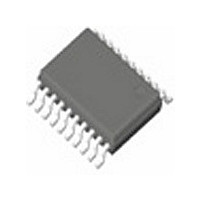
ICS85304AG-01LFT IDT, Integrated Device Technology Inc, ICS85304AG-01LFT Datasheet - Page 14

ICS85304AG-01LFT
Manufacturer Part Number
ICS85304AG-01LFT
Description
IC FANOUT BUFFER 1-5 20-TSSOP
Manufacturer
IDT, Integrated Device Technology Inc
Type
Fanout Buffer (Distribution), Multiplexerr
Series
HiPerClockS™r
Datasheet
1.ICS85304AG-01LFT.pdf
(15 pages)
Specifications of ICS85304AG-01LFT
Number Of Circuits
1
Ratio - Input:output
2:5
Differential - Input:output
Yes/Yes
Input
HCSL, LVDS, LVHSTL, LVPECL, SSTL
Output
LVPECL
Frequency - Max
650MHz
Voltage - Supply
3.135 V ~ 3.465 V
Operating Temperature
0°C ~ 70°C
Mounting Type
Surface Mount
Package / Case
20-TSSOP
Frequency-max
650MHz
Number Of Clock Inputs
2
Mode Of Operation
Differential
Output Frequency
650MHz
Output Logic Level
LVPECL
Operating Supply Voltage (min)
3.135V
Operating Supply Voltage (typ)
3.3V
Operating Supply Voltage (max)
3.465V
Package Type
TSSOP
Operating Temp Range
0C to 70C
Operating Temperature Classification
Commercial
Mounting
Surface Mount
Pin Count
20
Lead Free Status / RoHS Status
Lead free / RoHS Compliant
Other names
85304AG-01LFT
Revision History Sheet
IDT™ / ICS™ 3.3V LVPECL FANOUT BUFFER
ICS85304-01
LOW SKEW, 1-TO-5 DIFFERENTIAL-TO- 3.3V LVPECL FANOUT BUFFER
Rev
A
B
C
C
C
C
C
C
D
E
E
Table
T4B
T4D
T4D
T4D
T3B
T5
T5
T2
T9
T9
Page
14
10
13
4
5
5
5
5
3
3
3
8
6
7
1
2
4
6
8
9
8
9
3
Description of Change
V
V
Replaced tp
Replaced t
LVPECL DC Characteristics Table - added I
AC Characteristics Table - t
650ps max. to 700ps max.
Differential DC Characteristics Table - V
V
Revised Figure 1, CLK_EN Timing Diagram.
Revised Figure 1, CLK_EN Timing Diagram.
Revised Inputs heading from CLK or CLK, nPCLK or nPCLK to CLK or PCLK, nCLK or
nPCLK.
Added Termination for LVEPCL Output section.
3.3V Output Load Test Circuit Diagram - corrected V
Updated Output Rise/Fall Time Diagram.
Added Lead-Free bullet in Features section.
Pin Characteristics table - changed C
Absolute Maximum Ratings, updated Outputs rating.
Updated Parameter Measurement Information.
Added Differential Clock Input Interface section.
Added LVPECL Clock Input Interface section.
Ordering Information table - added Lead Free part number.
Per Document Errata, NEN-08-03, corrected name of PCLK/nPCLK to CLK1/nCLK1
Updated Differential Clock Input Interface section.
Deleted LVPECL Clock Input Interface section.
Added Recommendations for Unused Input and Output Pins section.
Power Considerations - corrected Junction Temperature calculations.
Ordering Information Table - corrected marking.
Updated format throughout the datasheet.
Corrected Figure 1, CLK_EN Timing Diagram.
V
with odc at values of 48% min., 50% typ., 52% max.
CMR
OH
CC.
V
and changed CLK/nCLK to CLK0/nCLK0 throughout the datasheet.
OL
EE
values changed from 1.9µA min. to V
values changed from 1.2µA min. to V
values changed from 1.5V min. to 0.5V min.; V
= -1.3V ± 0.165V.
PW
LH
and values of t
and tp
HL
with t
R
CYCLE
PD
and t
at the same values.
14
F
/2 - 40 min., t
values changed from 275ps min to 300ps min;
IN
CMR
4pF max. to 4pF typical.
CC
CC
IH
values changed from V
- 1.4µA min.; 2.3µA max. to V
- 2.0µA; 1.6µA max. to V
, I
IL
CYCLE
, V
PP
EE
DD
/2 typ., t
, and V
= -1.3V ± 0.135V to
max. to V
CMR
CYCLE
CC
rows.
CC
ICS85304AG-01 REV. E JULY 8, 2008
/2 + 40 max.
- 0.85V max.
CC
- 0.85V max. to
- 1.7µA max.
CC
- 1.0µA.
10/17/01
12/28/01
5/14/01
5/22/01
8/21/01
11/2/01
5/30/02
8/26/02
6/17/04
6/20/08
7/8/08
Date


