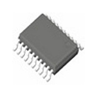
ICS85304AG-01LFT IDT, Integrated Device Technology Inc, ICS85304AG-01LFT Datasheet - Page 5

ICS85304AG-01LFT
Manufacturer Part Number
ICS85304AG-01LFT
Description
IC FANOUT BUFFER 1-5 20-TSSOP
Manufacturer
IDT, Integrated Device Technology Inc
Type
Fanout Buffer (Distribution), Multiplexerr
Series
HiPerClockS™r
Datasheet
1.ICS85304AG-01LFT.pdf
(15 pages)
Specifications of ICS85304AG-01LFT
Number Of Circuits
1
Ratio - Input:output
2:5
Differential - Input:output
Yes/Yes
Input
HCSL, LVDS, LVHSTL, LVPECL, SSTL
Output
LVPECL
Frequency - Max
650MHz
Voltage - Supply
3.135 V ~ 3.465 V
Operating Temperature
0°C ~ 70°C
Mounting Type
Surface Mount
Package / Case
20-TSSOP
Frequency-max
650MHz
Number Of Clock Inputs
2
Mode Of Operation
Differential
Output Frequency
650MHz
Output Logic Level
LVPECL
Operating Supply Voltage (min)
3.135V
Operating Supply Voltage (typ)
3.3V
Operating Supply Voltage (max)
3.465V
Package Type
TSSOP
Operating Temp Range
0C to 70C
Operating Temperature Classification
Commercial
Mounting
Surface Mount
Pin Count
20
Lead Free Status / RoHS Status
Lead free / RoHS Compliant
Other names
85304AG-01LFT
Table 4C. Differential DC Characteristics, V
NOTE 1: V
NOTE 2: Common mode input voltage is defined as V
Table 4D. LVPECL DC Characteristics, V
NOTE 1: Outputs terminated with 50
AC Electrical Characteristics
Table 5. AC Characteristics, V
All parameters measured at 500MHz unless noted otherwise
The cycle-to-cycle jitter on the input will equal the jitter on the output. The part does not add jitter.
NOTE 1: Measured from the differential input crossing point to the differential output crossing point.
NOTE 2: Defined as skew between outputs at the same supply voltage and with equal load conditions. Measured at the output differential
cross points.
NOTE 3: This parameter is defined in accordance with JEDEC Standard 65.
NOTE 4: Defined as skew between outputs on different devices operating at the same supply voltages and with equal load conditions.
Using the same type of inputs on each device, the outputs are measured at the differential cross points.
IDT™ / ICS™ 3.3V LVPECL FANOUT BUFFER
Symbol
I
I
V
V
Symbol
V
V
V
Parameter
f
t
tsk(o)
tsk(pp)
t
odc
IH
IL
MAX
PD
R
ICS85304-01
LOW SKEW, 1-TO-5 DIFFERENTIAL-TO- 3.3V LVPECL FANOUT BUFFER
PP
CMR
OH
OL
SWING
/ t
F
IL
Parameter
Output High Current; NOTE 1
Output Low Current; NOTE 1
Peak-to-Peak Output Voltage Swing
Parameter
Input High Current
Input Low Current
Peak-to-Peak Voltage; NOTE 1
Common Mode Input Voltage; NOTE 1, 2
should not be less than -0.3V
Symbol
Maximum Output Frequency
Propagation Delay; NOTE 1
Output Skew; NOTE 2, 3
Part-to-Part Skew; NOTE 3, 4
Output Rise/Fall Time
Output Duty Cycle
nCLK0, nCLK1
CLK0, CLK1
nCLK0, nCLK1
CLK0, CLK1
CC
Ω
= 3.3V ± 5%, V
to V
CC
– 2V.
CC
= 3.3V ± 5%, V
CC
IH
= 3.3V ± 5%, V
20% to 80% @ 50MHz
.
EE
Test Conditions
Test Conditions
=0V, T
V
V
ƒ ≤ 650MHz
CC
CC
V
V
Test Conditions
CC
CC
= 3.465V, V
= 3.465V, V
= V
= V
A
5
EE
= -40°C to 85°C
IN
IN
=0V, T
EE
= 3.465V
= 3.465V
=0V, T
IN
IN
A
= 0V
= 0V
= -40°C to 85°C
A
Minimum
V
V
= -40°C to 85°C
CC
CC
0.6
Minimum
Minimum
– 1.4
– 2.0
V
EE
300
1.0
48
-150
0.15
-5
+ 0.5
Typical
Typical
ICS85304AG-01 REV. E JULY 8, 2008
Typical
50
Maximum
V
V
Maximum
CC
CC
V
Maximum
0.85
CC
650
150
700
– 1.0
– 1.7
2.1
35
52
150
1.3
– 0.85
5
Units
Units
MHz
Units
µA
µA
V
ns
ps
ps
ps
%
µA
µA
µA
µA
V
V


