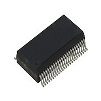
ICS9179BF-01LF IDT, Integrated Device Technology Inc, ICS9179BF-01LF Datasheet - Page 4

ICS9179BF-01LF
Manufacturer Part Number
ICS9179BF-01LF
Description
IC CLOCK BUFFER SDRAM 48-SSOP
Manufacturer
IDT, Integrated Device Technology Inc
Type
Fanout Buffer (Distribution)r
Specifications of ICS9179BF-01LF
Number Of Circuits
1
Ratio - Input:output
1:18
Differential - Input:output
No/No
Input
Clock
Output
Clock
Frequency - Max
150MHz
Voltage - Supply
3.135 V ~ 3.465 V
Operating Temperature
0°C ~ 70°C
Mounting Type
Surface Mount
Package / Case
48-SSOP
Frequency-max
150MHz
Number Of Outputs
18
Operating Supply Voltage (max)
3.465V
Operating Temp Range
0C to 70C
Propagation Delay Time
8ns
Operating Supply Voltage (min)
3.135V
Mounting
Surface Mount
Pin Count
48
Operating Supply Voltage (typ)
3.3V
Package Type
SSOP
Input Frequency
150MHz
Duty Cycle
55%
Operating Temperature Classification
Commercial
Lead Free Status / RoHS Status
Lead free / RoHS Compliant
Other names
9179BF-01LF
Available stocks
Company
Part Number
Manufacturer
Quantity
Price
ICS9179B-01
General I
A.
B.
C.
D.
E.
F.
G.
H.
Serial Configuration Command Bitmaps
Byte 0: SDRAM Clock Register
( A
( A
Notes: 1 = Enabled; 0 = Disabled, outputs held low
C
C
A
A
i B
i B
i B
i B
i B
i B
i B
i B
B
o l
o l
d
d
T I
: 6
: 6
7 t
6 t
5 t
4 t
3 t
2 t
0 t
1 t
d
d
k c
k c
e r
) 0
e r
) 0
D
D
For the clock generator to be addressed by an I
sequence, with an acknowledge bit between each byte.
The clock generator is a slave/receiver I
in the latches for verification. (set R/W# to 1 above). There is no BYTE count supported, so it does not meet
the Intel SMB PIIX4 protocol.
The data transfer rate supported by this clock generator is 100K bits/sec (standard mode)
The input is operating at 3.3V logic levels.
The data byte format is 8 bit bytes.
To simplify the clock generator I
bytes must be accessed in sequential order from lowest to highest byte with the ability to stop after any complete
byte has been transferred. The Command code and Byte count shown above must be sent, but the data is ignored
for those two bytes. The data is loaded until a Stop sequence is issued.
maintain all prior programming information.
At power-on, all registers are set to a default condition. Bytes 0 through 2 default to a 1 (Enabled output state).
In the power down mode (PWR_DWN# Low), the SDATA and SCLK pins are tristated and the internal data latches
P
G
s s
G
s s
1
1
1
1
N I
8
5
4
9
2
3
&
8
7
4
3
&
e
e
#
(
(
n
7 (
n
7 (
H
H
/ R
/ R
r e
r e
)
)
P
b
2
b
W
t a
t a
1
1
1
1
1
1
1
1
W
W
t i
t i
C serial interface information
D
) s
r o
r o
) s
#
#
S
A (
S
A (
S
A (
S
A (
S
A (
S
A (
S
A (
S
A (
D
D
D
D
D
D
D
D
c
c
c
c
c
c
c
c
D
R
R
R
R
R
R
R
R
/ t
/ t
/ t
/ t
/ t
/ t
/ t
/ t
E
A
A
A
A
A
A
A
A
A
A
n I
n I
n I
n I
n I
n I
n I
n I
S
M
M
M
M
M
M
M
M
C
a
a
a
a
a
a
a
a
C
C
7
c
6
c
5
c
4
c
3
c
2
c
1
c
0
c
R
) t
) t
) t
) t
) t
) t
) t
) t
K
P I
K
I T
O
N
c
+
d
o
B
m
u
c
8
y
o
m
m
e t
d
b
m
a
e
s t i
0
2
n
y
C interface, the protocol is set to use only block writes from the controller. The
d
2
A
A
C component. It can "read back "(in Philips I
C
C
K
K
d
Note: PWD = Power-Up Default
2
u
C controller, the following address must be sent as a start
4
+
m
B
c
m
8
y
o
e t
u
y
b
t n
s t i
B
1
y
e t
A
A
C
C
K
K
Byte 0, 1, 2, etc in sequence until STOP.
Then Byte 0, 1, 2, etc in
sequence until STOP.
2
C protocol) the data stored


