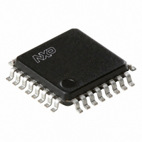
PCK940LBD,151 NXP Semiconductors, PCK940LBD,151 Datasheet - Page 9

PCK940LBD,151
Manufacturer Part Number
PCK940LBD,151
Description
IC CLOCK DISTR 1:18 32LQFP
Manufacturer
NXP Semiconductors
Type
Fanout Buffer (Distribution), Multiplexerr
Datasheet
1.PCK940LBD151.pdf
(16 pages)
Specifications of PCK940LBD,151
Number Of Circuits
1
Ratio - Input:output
1:18
Differential - Input:output
Yes/Yes
Input
LVCMOS, LVPECL
Output
LVCMOS
Frequency - Max
250MHz
Voltage - Supply
2.375 V ~ 3.465 V
Operating Temperature
0°C ~ 70°C
Mounting Type
Surface Mount
Package / Case
32-LQFP
Frequency-max
250MHz
Lead Free Status / RoHS Status
Lead free / RoHS Compliant
Other names
568-3642-5
935281611151
PCK940LBD-S
935281611151
PCK940LBD-S
Available stocks
Company
Part Number
Manufacturer
Quantity
Price
Company:
Part Number:
PCK940LBD,151
Manufacturer:
NXP Semiconductors
Quantity:
10 000
Philips Semiconductors
PCK940L_1
Product data sheet
Fig 3. Propagation delay (t
Fig 5. Output duty cycle
Fig 7. Transition time test reference
(1) output 2.4 V; input 2.0 V (V
(2) output 0.55 V; input 0.8 V (V
PECL_CLK
PECL_CLK
The time from the PLL controlled edge to the
non-controlled edge, divided by the time between
PLL controlled edges, expressed as a percentage.
output 1.8 V; input 1.7 V (V
output 0.6 V; input 0.7 V (V
o
Qn
= (t
p
9.1 Timing diagrams
T
o
t
V
p
t
i(p-p)
PD
100 %)
T
o
PD
) test reference
CC
CC
CC
CC
= 3.3 V)
= 2.5 V)
= 2.5 V)
= 3.3 V)
002aab291
V
0.5V
GND
CC
002aab893
CC
V
0.5V
GND
V
CC
ICR
Rev. 01 — 4 April 2006
t
f
CC
t
Fig 4. LVCMOS_CLK propagation delay (t
Fig 6. Output-to-output skew
r
002aab292
LVCMOS_CLK
reference
The pin-to-pin skew is defined as the worst-case
difference in propagation delay between any two
similar delay paths within a single device.
(2)
(1)
Low voltage 1 : 18 clock distribution chip
Qn
t
PD
© Koninklijke Philips Electronics N.V. 2006. All rights reserved.
t
sk(o)
PCK940L
002aab891
PD
002aab892
V
0.5V
GND
V
0.5V
GND
CC
CC
) test
V
0.5V
GND
V
0.5V
GND
CC
CC
CC
CC
CC
CC
9 of 16


