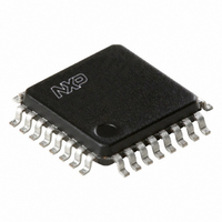
PCK2111BD,151 NXP Semiconductors, PCK2111BD,151 Datasheet - Page 4

PCK2111BD,151
Manufacturer Part Number
PCK2111BD,151
Description
IC CLOCK DISTRIB LVDS 32LQFP
Manufacturer
NXP Semiconductors
Type
Fanout Buffer (Distribution), Multiplexerr
Datasheet
1.PCK2111BD157.pdf
(9 pages)
Specifications of PCK2111BD,151
Package / Case
32-LQFP
Number Of Circuits
1
Ratio - Input:output
2:10
Differential - Input:output
Yes/Yes
Input
LVDS
Output
LVDS
Frequency - Max
800MHz
Voltage - Supply
2.375 V ~ 2.625 V
Operating Temperature
-40°C ~ 85°C
Mounting Type
Surface Mount
Frequency-max
800MHz
Mounting Style
SMD/SMT
Lead Free Status / RoHS Status
Lead free / RoHS Compliant
Other names
935271528151
PCK2111BD-S
PCK2111BD-S
PCK2111BD-S
PCK2111BD-S
Available stocks
Company
Part Number
Manufacturer
Quantity
Price
Company:
Part Number:
PCK2111BD,151
Manufacturer:
NXP Semiconductors
Quantity:
10 000
Philips Semiconductors
ABSOLUTE MAXIMUM RATINGS
Absolute Maximum Ratings are those values beyond which damage to the device may occur.
Functional operation under these conditions is not implied.
RECOMMENDED OPERATING CONDITIONS
DC ELECTRICAL CHARACTERISTICS
T
NOTES:
1. All currents into device pins are positive; all currents out of device pins are negative. All voltages are referenced to device ground unless
2. All typical values are given for V
3. C
4. Generator waveforms for all tests unless otherwise specified: f = 1 MHz, Z
5. The PCK2111 is a current mode device, and only functions to datasheet specifications when a resistive load is applied to the drives outputs.
2002 Dec 16
Driver
Receiver
Device
amb
SYMBOL
SYMBOL
SYMBOL
1:10 LVDS clock distribution device
otherwise specified.
∆V
∆V
C
I
ESD
T
I
V
I
V
V
V
V
V
V
C
OSD
V
OSD
CCD
V
L
V
I
amb
= -40 °C to +85 °C unless otherwise specified; V
OUT
T
IDH
CC
CC
OD
OS
IDL
IN
I
BB
IR
IN
IH
IL
OD
OS
I
includes probe and fixture capacitance.
j
Supply voltage
Driver short circuit current
Electrostatic discharge (Human Body Model 1.5 kΩ, 100 pF)
Junction temperature
Supply voltage
Receiver input voltage
Operating ambient temperature range in free air
Output differential voltage
V
Offset voltage
V
Output short circuit current
Input threshold HIGH
Input threshold LOW
Input current
Output reference voltage
Power supply current
Input capacitance
Output capacitance
Logic input HIGH threshold
Logic input LOW threshold
Logic input current
OD
OS
magnitude change
magnitude change
PARAMETER
CC
= +2.5 V and T
PARAMETER
PARAMETER
amb
CC
= 2.5 V ±5% (Notes 1, 2)
= +25 °C, unless otherwise specified.
All drivers enabled and loaded;
input frequency = 800 MHz
V
V
I
IN
CONDITIONS
IN
V
OUT
V
V
V
R
R
R
R
= V
V
V
CC
V
CC
4
CC
CC
V
= 0 V to V
L
L
L
L
OD
IN
IN
O
≤ 100 µA
= 100 Ω
= 100 Ω
= 100 Ω
= 100 Ω
= 2.5 V;
CC
= 2.5 V;
= 2.5 V
= 2.5 V
= V
= 0 V
= 0 V
= 0 V
or GND
O
CC
= 50 Ω, 50% duty cycle.
CC
1.125
-100
1.15
MIN
250
—
—
—
—
—
—
—
—
—
—
—
—
2
2.375
TYP
GND
1.25
1.25
MIN
-40
350
190
15
50
50
—
—
—
—
—
—
—
7
5
5
continuous
-0.3 to 2.8
2
LIMITS
150
>2
2.625
1.375
MAX
MAX
PCK2111
V
1.35
+85
450
100
100
100
230
±10
0.8
50
50
40
15
—
—
—
—
CC
Product data
UNIT
UNIT
UNIT
mV
mV
mV
mA
mA
mV
mV
mA
µA
µA
µA
kV
°C
°C
pF
pF
V
V
V
V
V
V


