ICS853111BYLF IDT, Integrated Device Technology Inc, ICS853111BYLF Datasheet - Page 8
ICS853111BYLF
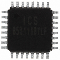
Manufacturer Part Number
ICS853111BYLF
Description
IC FANOUT BUFF LVPECL/ECL 32TQFP
Manufacturer
IDT, Integrated Device Technology Inc
Series
HiPerClockS™r
Type
Fanout Buffer (Distribution), Multiplexerr
Datasheet
1.ICS853111BYLF.pdf
(19 pages)
Specifications of ICS853111BYLF
Number Of Circuits
1
Ratio - Input:output
2:10
Differential - Input:output
Yes/Yes
Input
CML, LVDS, LVPECL, SSTL
Output
ECL, LVPECL
Frequency - Max
3GHz
Voltage - Supply
2.375 V ~ 3.8 V
Operating Temperature
-40°C ~ 85°C
Mounting Type
Surface Mount
Package / Case
32-TQFP, 32-VQFP
Frequency-max
3GHz
Lead Free Status / RoHS Status
Lead free / RoHS Compliant
Other names
800-1165
853111BYLF
853111BYLF
Available stocks
Company
Part Number
Manufacturer
Quantity
Price
Company:

Part Number:
ICS853111BYLF
Manufacturer:
ICS
Quantity:
1 235
Company:
Part Number:
ICS853111BYLF
Manufacturer:
IDT, Integrated Device Technology Inc
Quantity:
10 000
Company:
Part Number:
ICS853111BYLFT
Manufacturer:
IDT, Integrated Device Technology Inc
Quantity:
10 000


Figure 2A shows how the differential input can be wired to accept
single ended levels. The reference voltage V_REF ~ V
generated by the bias resistors R1, R2 and C1. This bias circuit
should be located as close as possible to the input pin. The ratio
W
Figure 2B shows an example of the differential input that can
be wired to accept single ended LVPECL levels. The reference
voltage level V
IDT
W
ICS853111B
LOW SKEW, 1-TO-10, DIFFERENTIAL-TO-2.5V, 3.3V LVPECL/ECL FANOUT BUFFER
IRING THE
IRING THE
™
/ ICS
™
1-TO-10, LVPECL/ECL FANOUT BUFFER
D
D
BB
IFFERENTIAL
IFFERENTIAL
generated from the device is connected to the
F
IGURE
I
I
NPUT TO
NPUT TO
2B. S
F
IGURE
INGLE
A
Single Ended Clock Input
A
A
PPLICATION
CCEPT
CCEPT
2A. S
E
NDED
INGLE
S
S
INGLE
LVPECL S
INGLE
CLK_IN
0.1uF
C1
0.1u
E
C1
NDED
CC
/2 is
E
V_REF
E
NDED
NDED
I
S
NFORMATION
IGNAL
IGNAL
8
LVPECL L
LVCMOS L
of R1 and R2 might need to be adjusted to position the V_REF in
the center of the input voltage swing. For example, if the input
clock swing is only 2.5V and V
and R2/R1 = 0.609.
negative input. The C1 capacitor should be located as close as
possible to the input pin.
R1
1K
R2
1K
D
D
+
VBB
-
RIVING
V
RIVING
CC
VDD(or VCC)
PCLKx
nPCLKx
D
D
IFFERENTIAL
IFFERENTIAL
EVELS
EVELS
I
ICS853111BY REV. B SEPTEMBER 5, 2007
I
NPUT
NPUT
CC
= 3.3V, V_REF should be 1.25V
Related parts for ICS853111BYLF
Image
Part Number
Description
Manufacturer
Datasheet
Request
R

Part Number:
Description:
TRANSLATION DEVICE DPI 80-PQFP
Manufacturer:
IDT, Integrated Device Technology Inc
Datasheet:
Part Number:
Description:
IDT PART
Manufacturer:
IDT, Integrated Device Technology Inc
Datasheet:
Part Number:
Description:
IC LIU T1/E1/J1 OCTAL 256PBGA
Manufacturer:
IDT, Integrated Device Technology Inc
Datasheet:

Part Number:
Description:
IC FREQ TIMING GENERATOR 28TSSOP
Manufacturer:
IDT, Integrated Device Technology Inc
Datasheet:
Part Number:
Description:
IC CLK DVR PLL 1:10 40VFQFPN
Manufacturer:
IDT, Integrated Device Technology Inc
Datasheet:
Part Number:
Description:
IC CLK FANOUT BUFFER 1:18 32LQFP
Manufacturer:
IDT, Integrated Device Technology Inc
Datasheet:
Part Number:
Description:
IC CLK FANOUT BUFFER 1:18 32LQFP
Manufacturer:
IDT, Integrated Device Technology Inc
Datasheet:
Part Number:
Description:
IC CK505 VREG/RES 56TSSOP
Manufacturer:
IDT, Integrated Device Technology Inc
Datasheet:

Part Number:
Description:
IC SDRAM CLK DVR 1:10 48-TSSOP
Manufacturer:
IDT, Integrated Device Technology Inc
Datasheet:

Part Number:
Description:
IC CLK DVR PLL 1:10 48TSSOP
Manufacturer:
IDT, Integrated Device Technology Inc
Datasheet:
Part Number:
Description:
IC FLEXPC CLK PROGR P4 56-TSSOP
Manufacturer:
IDT, Integrated Device Technology Inc
Datasheet:
Part Number:
Description:
IC FLEXPC CLK PROGR P4 56-TSSOP
Manufacturer:
IDT, Integrated Device Technology Inc
Datasheet:
Part Number:
Description:
IC FLEXPC CLK PROGR P4 56-SSOP
Manufacturer:
IDT, Integrated Device Technology Inc
Datasheet:

Part Number:
Description:
IC PLL CLK DRIVER 2.5V 28-TSSOP
Manufacturer:
IDT, Integrated Device Technology Inc
Datasheet:
Part Number:
Description:
IC CLOCK DRIVER 2.5V 24-TSSOP
Manufacturer:
IDT, Integrated Device Technology Inc
Datasheet: