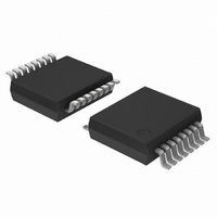
74HCT4046ADB,112 NXP Semiconductors, 74HCT4046ADB,112 Datasheet - Page 12

74HCT4046ADB,112
Manufacturer Part Number
74HCT4046ADB,112
Description
IC PLL W/VCO 16-SSOP
Manufacturer
NXP Semiconductors
Type
Phase Lock Loop (PLL)r
Series
74HCTr
Datasheets
1.74HCT4046AD112.pdf
(34 pages)
2.74HCT4046ADB112.pdf
(19 pages)
3.74HCT4046ADB112.pdf
(23 pages)
Specifications of 74HCT4046ADB,112
Number Of Circuits
1
Package / Case
16-SSOP
Pll
Yes
Input
Clock
Output
Clock
Ratio - Input:output
2:3
Differential - Input:output
No/No
Frequency - Max
19MHz
Divider/multiplier
No/No
Voltage - Supply
4.5 V ~ 5.5 V
Operating Temperature
-40°C ~ 125°C
Mounting Type
Surface Mount
Frequency-max
19MHz
Supply Voltage (max)
5.5 V
Supply Voltage (min)
4.5 V
Maximum Operating Temperature
+ 125 C
Minimum Operating Temperature
- 40 C
Input Level
CMOS
Mounting Style
SMD/SMT
Operating Supply Voltage
4.5 V to 5.5 V
Output Level
CMOS
Lead Free Status / RoHS Status
Lead free / RoHS Compliant
Lead Free Status / RoHS Status
Lead free / RoHS Compliant, Lead free / RoHS Compliant
Other names
568-2853-5
935174940112
935174940112
Philips Semiconductors
Test circuit for 74HC
HCT TYPES
AC waveforms 74HCT
March 1988
handbook, full pagewidth
HCMOS family characteristics
Switch position
Note
1. For open-drain N-channel outputs t
TEST
t
t
t
t
C
R
PZH
PZL
PHZ
PLZ
L
T
=
=
Fig.8 Input rise and fall times, transition times and propagation delays for combinatorial logic ICs.
load capacitance including jig and probe capacitance
(see AC CHARACTERISTICS for values).
termination resistance should be equal to the output impedance Z
the pulse generator.
SWITCH
GND
V
GND
V
CC
CC
handbook, halfpage
GENERATOR
PULSE
INPUT
OUTPUT
Fig.7 Test circuit for 3-state outputs.
PLZ
and t
V I
t PHL
t THL
10%
90%
PZL
R T
t r
1.3 V
are applicable.
90%
1.3 V
10%
D.U.T
V CC
12
o
of
t f
V O
C L
t PLH
t TLH
R L = 1 k
50 pF
MGK567
FAMILY SPECIFICATIONS
3 V
GND
MGK563
V CC


