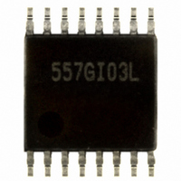
ICS557GI-03LF IDT, Integrated Device Technology Inc, ICS557GI-03LF Datasheet - Page 3

ICS557GI-03LF
Manufacturer Part Number
ICS557GI-03LF
Description
IC CLOCK SOURCE PCI 16-TSSOP
Manufacturer
IDT, Integrated Device Technology Inc
Type
Clock Generatorr
Specifications of ICS557GI-03LF
Input
Clock, Crystal
Output
HCSL, LVDS
Frequency - Max
200MHz
Voltage - Supply
2.97 V ~ 3.63 V
Operating Temperature
-40°C ~ 85°C
Mounting Type
Surface Mount
Package / Case
16-TSSOP
Frequency-max
200MHz
Number Of Elements
1
Supply Current
78mA
Pll Input Freq (min)
25MHz
Operating Supply Voltage (typ)
3.3V
Operating Temp Range
-40C to 85C
Package Type
TSSOP
Output Frequency Range
25 to 200MHz
Operating Supply Voltage (min)
2.97V
Operating Supply Voltage (max)
3.63V
Operating Temperature Classification
Industrial
Pin Count
16
Lead Free Status / RoHS Status
Lead free / RoHS Compliant
Other names
557GI-03LF
800-1066
800-1066-5
800-1066
800-1066
800-1066-5
800-1066
Available stocks
Company
Part Number
Manufacturer
Quantity
Price
Part Number:
ICS557GI-03LF
Manufacturer:
IDT
Quantity:
20 000
Applications Information
External Components
A minimum number of external components are required for
proper operation.
Decoupling Capacitors
Decoupling capacitors of 0.01 µF should be connected
between each VDD pin and the ground plane, as close to
the VDD pin as possible. Do not share ground vias between
components. Route power from power source through the
capacitor pad and then into ICS pin.
Crystal
A 25 MHz fundamental mode parallel resonant crystal
should be used. This crystal must have less than 300 ppm
of error across temperature in order for the ICS557-03 to
meet PCI Express specifications.
Crystal Capacitors
Crystal capacitors are connected from pins X1 to ground
and X2 to ground to optimize the accuracy of the output
frequency.
C
Crystal Capacitors (pF) = (C
For example, for a crystal with a 16 pF load cap, each
external crystal cap would be 16 pF. (16-8)*2=16.
Current Source (Iref) Reference Resistor - R
If board target trace impedance (Z) is 50Ω , then R
(1%), providing IREF of 2.32 mA. The output current (I
equal to 6*IREF.
Output Termination
The PCI-Express differential clock outputs of the ICS557-03
are open source drivers and require an external series
resistor and a resistor to ground. These resistor values and
their allowable locations are shown in detail in the
PCI-Express Layout Guidelines section.
The ICS557-03 can also be configured for LVDS compatible
voltage levels. See the LVDS Compatible Layout
Guidelines section.
IDT™ / ICS™ PCI-EXPRESS GEN1 CLOCK SOURCE
L
ICS557-03
PCI-EXPRESS GEN1 CLOCK SOURCE
= Crystal’s load capacitance in pF
L
- 8) * 2
R
R
= 475Ω
OH
) is
3
Output Structures
General PCB Layout Recommendations
For optimum device performance and lowest output phase
noise, the following guidelines should be observed.
1. Each 0.01µF decoupling capacitor should be mounted on
the component side of the board as close to the VDD pin as
possible.
2. No vias should be used between decoupling capacitor
and VDD pin.
3. The PCB trace to VDD pin should be kept as short as
possible, as should the PCB trace to the ground via.
Distance of the ferrite bead and bulk decoupling from the
device is less critical.
4. An optimum layout is one with all components on the
same side of the board, minimizing vias through other signal
layers (any ferrite beads and bulk decoupling capacitors can
be mounted on the back). Other signal traces should be
routed away from the ICS557-03.This includes signal traces
just underneath the device, or on layers adjacent to the
ground plane layer used by the device.
R
=2.3 mA
R
IREF
475
Ω
See Output Termination
Sections - Pages 3 ~ 5
ICS557-03
6*IREF
PCIE SSCG
REV M 042709


