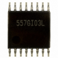
ICS557GI-03LF IDT, Integrated Device Technology Inc, ICS557GI-03LF Datasheet - Page 7

ICS557GI-03LF
Manufacturer Part Number
ICS557GI-03LF
Description
IC CLOCK SOURCE PCI 16-TSSOP
Manufacturer
IDT, Integrated Device Technology Inc
Type
Clock Generatorr
Specifications of ICS557GI-03LF
Input
Clock, Crystal
Output
HCSL, LVDS
Frequency - Max
200MHz
Voltage - Supply
2.97 V ~ 3.63 V
Operating Temperature
-40°C ~ 85°C
Mounting Type
Surface Mount
Package / Case
16-TSSOP
Frequency-max
200MHz
Number Of Elements
1
Supply Current
78mA
Pll Input Freq (min)
25MHz
Operating Supply Voltage (typ)
3.3V
Operating Temp Range
-40C to 85C
Package Type
TSSOP
Output Frequency Range
25 to 200MHz
Operating Supply Voltage (min)
2.97V
Operating Supply Voltage (max)
3.63V
Operating Temperature Classification
Industrial
Pin Count
16
Lead Free Status / RoHS Status
Lead free / RoHS Compliant
Other names
557GI-03LF
800-1066
800-1066-5
800-1066
800-1066
800-1066-5
800-1066
Available stocks
Company
Part Number
Manufacturer
Quantity
Price
Part Number:
ICS557GI-03LF
Manufacturer:
IDT
Quantity:
20 000
AC Electrical Characteristics - CLK0/CLK1, CLK0/CLK1
Unless stated otherwise, VDD=3.3 V ±10%, Ambient Temperature -40 to +85° C
Electrical Characteristics - Differential Phase Jitter
IDT™ / ICS™ PCI-EXPRESS GEN1 CLOCK SOURCE
Input Frequency
Output Frequency
Output High Voltage
Output Low Voltage
Crossing Point Voltage
Crossing Point Voltage
Jitter, Cycle-to-Cycle
Frequency Synthesis Error
Modulation Frequency
Rise Time
Fall Time
Rise/Fall Time Variation
Output to Output Skew
Duty Cycle
Output Enable Time
Output Disable Time
Stabilization Time
Spread Spectrum Transition
Time
ICS557-03
PCI-EXPRESS GEN1 CLOCK SOURCE
Jitter, Phase
Parameter
Note 1: Test setup is R
Note 2: Measurement taken from a single-ended waveform.
Note 3: Measurement taken from a differential waveform.
Note 4: Measured at the crossing point where instantaneous voltages of both CLK and CLK are equal.
Note 5: CLK pins are tri-stated when OE is low asserted. CLK is driven differential when OE is high.
Note 1: Guaranteed by design and characterization, not 100% tested in production.
Note 2: See http://www.pcisig.com for complete specs.
Parameter
1,2
1,2
1,3
1,2
1,2
5
5
1,3
1,2
1,2,4
1,2
t
Symbol
jphasePLL
L
Symbol
=50 ohms with 2 pF, Rr = 475Ω (1%).
t
t
SPREAD
STABLE
V
V
t
t
OR
OF
OH
OL
HCSL termination
LVDS termination
HCSL
HCSL
Absolute
Variation over all edges
All outputs
Spread spectrum
From 0.175 V to 0.525 V
From 0.525 V to 0.175 V
All outputs
All outputs
From power-up VDD=3.3 V
Stabilization time after spread
spectrum changes
Conditions
PCIe Gen 1
Conditions
7
Min
-
Typ
-
Min.
-150
660
250
175
175
25
25
45
30
Max
86
Typ.
31.5
700
350
332
344
3.0
3.0
25
80
10
10
0
0
ps (p-p)
Units
ICS557-03
Max.
200
100
850
550
140
700
700
125
3.5
3.5
27
33
50
55
12
12
Notes
1, 2
PCIE SSCG
REV M 042709
Units
MHz
MHz
MHz
ppm
kHz
mV
mV
mV
mV
ms
ms
ps
ps
ps
ps
ps
µs
µs
%


