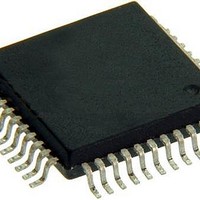
CY7B9945V-5AXC Cypress Semiconductor Corp, CY7B9945V-5AXC Datasheet - Page 7

CY7B9945V-5AXC
Manufacturer Part Number
CY7B9945V-5AXC
Description
IC CLK BUFF 11OUT 200MHZ 52LQFP
Manufacturer
Cypress Semiconductor Corp
Type
Clock Buffer, Fanout Distributionr
Series
RoboClock™r
Datasheet
1.CY7B9945V-5AXC.pdf
(13 pages)
Specifications of CY7B9945V-5AXC
Number Of Circuits
1
Package / Case
52-LQFP
Pll
Yes
Input
LVPECL, LVTTL
Output
LVTTL
Ratio - Input:output
4:10
Differential - Input:output
Yes/No
Frequency - Max
200MHz
Divider/multiplier
Yes/Yes
Voltage - Supply
2.97 V ~ 3.63 V
Operating Temperature
0°C ~ 70°C
Mounting Type
Surface Mount
Frequency-max
200MHz
Maximum Input Frequency
200 MHz
Minimum Input Frequency
24 MHz
Output Frequency Range
24 MHz to 200 MHz
Supply Voltage (max)
3.63 V
Supply Voltage (min)
2.97 V
Maximum Operating Temperature
+ 70 C
Minimum Operating Temperature
0 C
Mounting Style
SMD/SMT
Operating Supply Voltage
3.3 V
Lead Free Status / RoHS Status
Lead free / RoHS Compliant
Available stocks
Company
Part Number
Manufacturer
Quantity
Price
Company:
Part Number:
CY7B9945V-5AXC
Manufacturer:
Cypress Semiconductor Corp
Quantity:
10 000
Company:
Part Number:
CY7B9945V-5AXCT
Manufacturer:
Cypress Semiconductor Corp
Quantity:
10 000
Lock Detect Output Description
The LOCK detect output indicates the lock condition of the
integrated PLL. Lock detection is accomplished by comparing
the phase difference between the reference and feedback
inputs. Phase error is declared when the phase difference
between the two inputs is greater than the specified device
propagation delay limit t
When in the locked state, after four or more consecutive
feedback clock cycles with phase errors, the LOCK output is
forced LOW to indicate out-of-lock state.
When in the out-of-lock state, 32 consecutive phase errorless
feedback clock cycles are required to enable the LOCK output to
indicate lock condition (LOCK = HIGH).
If the feedback clock is removed after LOCK has gone HIGH, a
“Watchdog” circuit is implemented to indicate the out-of-lock
condition after a time-out period by deasserting LOCK LOW. This
time out period is based upon a divided down reference clock.
This assumes that there is activity on the selected REF input. If
there is no activity on the selected REF input then the LOCK
detect pin does not accurately reflect the state of the internal
PLL.
Factory Test Mode Description
The device enters factory test mode when the MODE is driven
to MID. In factory test mode, the device operates with its internal
PLL disconnected; input level supplied to the reference input is
used in place of the PLL output. In TEST mode the FB input is
tied LOW. All functions of the device remain operational in
factory test mode except the internal PLL and output bank
disables. The MODE input is designed as a static input. Dynam-
ically toggling this input from LOW to HIGH temporarily causes
the device to go into factory test mode (when passing through
the MID state).
When in the test mode, the device is reset to a deterministic state
by driving the DIS2 input HIGH. Doing so disables all outputs
and, after the selected reference clock pin has five positive
transitions, all internal finite state machines (FSM) are set at a
deterministic state. The states depend on the configurations of
Document Number: 38-07336 Rev. *H
PD
.
PRELIMINARY
the divide, skew and frequency selection. All clock outputs stay
in High-Z mode and all FSMs stay in the deterministic state until
DIS2 is deasserted. This causes the device to reenter factory
test mode.
Safe Operating Zone
Figure 3
exceeding its allowable maximum junction temperature of
150°C.
operate at 185 MHz (with 25 pF load and no air flow) or 200 MHz
(with 10-pF load and no air flow) at various ambient tempera-
tures. At the limit line, all other outputs are configured to
divide-by-two (i.e., operating at 92.5 MHz) or lower frequencies.
The device operates below maximum allowable junction temper-
ature of 150°C when its configuration (with the specified
constraints) falls within the shaded region (safe operating zone).
Figure 3
that can operate at 200 MHz is 6.
Figure 3. Typical Safe Operating Zone
100
Figure 3
95
90
85
80
75
70
65
60
55
50
shows that at 85°C, the maximum number of outputs
shows the operating condition of the device not
2
Number of Outputs at 185 MHz
shows the maximum number of outputs that can
Typical Safe Operating Zone
(25-pF Load, 0-m/s air flow)
Safe Operating Zone
4
6
8
RoboClock
CY7B9945V
10
Page 7 of 13
[+] Feedback


