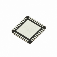
SI5317D-C-GM Silicon Laboratories Inc, SI5317D-C-GM Datasheet - Page 12

SI5317D-C-GM
Manufacturer Part Number
SI5317D-C-GM
Description
IC CLK JITTER CLEANR PROG 36QFN
Manufacturer
Silicon Laboratories Inc
Type
Jitter Cleanerr
Series
Si5317r
Datasheet
1.SI5317C-C-GM.pdf
(46 pages)
Specifications of SI5317D-C-GM
Package / Case
36-QFN
Pll
Yes with Bypass
Input
Clock, Crystal
Output
CML, CMOS, LVDS, LVPECL
Number Of Circuits
1
Ratio - Input:output
1:2
Differential - Input:output
Yes/Yes
Frequency - Max
100MHz
Divider/multiplier
No/No
Voltage - Supply
1.71 V ~ 3.63 V
Operating Temperature
-40°C ~ 85°C
Mounting Type
Surface Mount
Frequency-max
100MHz
Termination Style
SMD/SMT
Output Format
CML
Dimensions
5 mm W x 7 mm L x 1.85 mm H
Minimum Operating Temperature
- 40 C
Maximum Operating Temperature
+ 85 C
Mounting Style
SMD/SMT
Product
XO
Frequency
10 MHz to 945 MHz
Frequency Stability
+/- 20 PPM
Supply Voltage
3.3 Volts
Height
1.85 mm
Lead Free Status / RoHS Status
Lead free / RoHS Compliant
Lead Free Status / RoHS Status
Lead free / RoHS Compliant, Lead free / RoHS Compliant
Other names
336-1920
Si5317
Table 5. Performance Specifications
(V
12
Table 4. AC Characteristics (Continued)
(V
Jitter Generation
LVPECL output format
BW = 120 Hz
Phase Noise
f
LVPECL output format
Notes:
LVCMOS Output Pins
Rise/Fall Times
LOSn Trigger Window
Time to Clear LOL after LOS Cleared t
PLL Performance
Lock Time
Closed Loop Jitter Peaking
Jitter Tolerance
Minimum Reset Pulse Width
Spurious Noise
Phase Change due to Temperature
Variation
f
IN
IN
DD
DD
= f
1. BWSEL [1:0] loop bandwidth settings provided in Table 9 on page 22.
2. 114.285 MHz 3rd OT crystal used as XA/XB input.
3. V
4. T
5. Test condition: f
= f
= 1.8 ±5%, 2.5 ±10%, or 3.3 V ±10%, T
= 1.8 ±5%, 2.5 ±10%, or 3.3 V ±10%, T
OUT
OUT
(20-80%), LVPECL clock output.
Parameter
A
DD
= 85 °C
= 622.08 MHz
= 622.08 MHz,
= 2.5 V
Parameter
IN
= 622.08 MHz, f
Symbol
CKO
J
GEN
PN
OUT
LOS
t
Symbol
SP
t
LOCKHW
A
A
CLRLOL
RSTMIN
t
J
TEMP
= 622.08 MHz, LVPECL clock input: 1.19 Vppd with 0.5 ns rise/fall time
= –40 to 85 ºC)
= –40 to 85 ºC)
J
t
1, 2, 3, 4, 5
TOL
SPUR
RF
PK
TRIG
50 kHz–80 MHz
12 kHz–20 MHz
800 Hz–80 MHz
Test Condition
100 kHz offset
10 kHz offset
1 MHz offset
1 kHz offset
are changed, with valid CKIN
RATE, BWSEL, or FRQSEL
From last CKIN to LOS
Whenever RST, FRQTBL,
f
Max phase changes from
(n > 1, n x f3 < 100 MHz)
in
to LOL; BW = 100 Hz
Rev. 1.1
unchanged and XA/XB
BW determined by
Max spur @ n x f3
LOS to LOL
Test Condition
CLOAD = 20 pf
–40 to +85 ºC
See Figure 2
BWSEL[1:0]
stable.
Min
—
—
—
—
—
—
—
5000/
Min
BW
—
—
—
—
—
—
1
–132
–132
–106
–121
0.32
0.31
Typ
0.4
0.05
Typ
–93
300
25
10
—
—
—
–100
–104
–119
Max
0.42
0.41
0.45
–87
Max
750
–70
500
1.2
0.1
—
—
—
—
ns pk-
Units
dBc/Hz
dBc/Hz
dBc/Hz
dBc/Hz
ps rms
ps rms
ps rms
dBc
sec
ms
dB
Unit
ns
µs
pk
µs
ps


