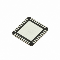
SI5317D-C-GM Silicon Laboratories Inc, SI5317D-C-GM Datasheet - Page 36

SI5317D-C-GM
Manufacturer Part Number
SI5317D-C-GM
Description
IC CLK JITTER CLEANR PROG 36QFN
Manufacturer
Silicon Laboratories Inc
Type
Jitter Cleanerr
Series
Si5317r
Datasheet
1.SI5317C-C-GM.pdf
(46 pages)
Specifications of SI5317D-C-GM
Package / Case
36-QFN
Pll
Yes with Bypass
Input
Clock, Crystal
Output
CML, CMOS, LVDS, LVPECL
Number Of Circuits
1
Ratio - Input:output
1:2
Differential - Input:output
Yes/Yes
Frequency - Max
100MHz
Divider/multiplier
No/No
Voltage - Supply
1.71 V ~ 3.63 V
Operating Temperature
-40°C ~ 85°C
Mounting Type
Surface Mount
Frequency-max
100MHz
Termination Style
SMD/SMT
Output Format
CML
Dimensions
5 mm W x 7 mm L x 1.85 mm H
Minimum Operating Temperature
- 40 C
Maximum Operating Temperature
+ 85 C
Mounting Style
SMD/SMT
Product
XO
Frequency
10 MHz to 945 MHz
Frequency Stability
+/- 20 PPM
Supply Voltage
3.3 Volts
Height
1.85 mm
Lead Free Status / RoHS Status
Lead free / RoHS Compliant
Lead Free Status / RoHS Status
Lead free / RoHS Compliant, Lead free / RoHS Compliant
Other names
336-1920
Si5317
9. Pin Descriptions: Si5317
Note: Pin assignments are preliminary and subject to change.
36
5, 10, 32
Pin #
1
2
3
Pin Name
FRQTBL
RST
LOS
V
DD
V
I/O
O
DD
I
I
FRQTBL
Table 14. Si5317 Pin Descriptions
GND
VDD
RST
LOS
Signal Level
NC
NC
XA
XB
LVCMOS
LVCMOS
3-level
Supply
1
2
3
4
5
6
7
8
9
36
10 11 12 13 14 15 16 17
35
34
33
nal, the Si5317 will perform an internal self-calibration when
a valid input signal is present.
This pin has a weak pull-up.
Frequency Table.
Selects frequency table.
This pin has a weak pull-up and weak pull-down and defaults
to M. Some designs may require an external resistor voltage
divider when driven by an active device that will tri-state.
CKIN Loss of Signal.
Active high loss-of-signal indicator for CKIN. Once triggered,
the alarm will remain active until CKIN is validated.
0 = CKIN present
1 = LOS on CKIN
Supply.
The device operates from a 1.8, 2.5, or 3.3 V supply. Bypass
capacitors should be associated with the following V
5
10
32
A 1.0 µF should also be placed as close to device as is
practical.
GND
External Reset.
Active low input that performs external hardware reset of
device. Resets all internal logic to a known state. Clock out-
puts are tristated during reset. After rising edge of RST sig-
Pad
Rev. 1.1
32
31
30
29
28
18
27
26
25
24
23
22
21
20
19
0.1 µF
0.1 µF
0.1 µF
FRQSEL3
FRQSEL2
FRQSEL1
FRQSEL0
BWSEL1
BWSEL0
NC
INC
DEC
Description
DD
pins:


