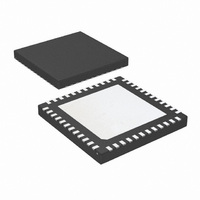
LMK03000CISQ/NOPB National Semiconductor, LMK03000CISQ/NOPB Datasheet - Page 20

LMK03000CISQ/NOPB
Manufacturer Part Number
LMK03000CISQ/NOPB
Description
IC CLOCK CONDITIONER PREC 48-LLP
Manufacturer
National Semiconductor
Type
Clock Conditionerr
Datasheet
1.LMK03000DISQENOPB.pdf
(30 pages)
Specifications of LMK03000CISQ/NOPB
Pll
Yes
Input
Clock
Output
LVDS, LVPECL
Number Of Circuits
1
Ratio - Input:output
1:8
Differential - Input:output
Yes/Yes
Frequency - Max
1.296GHz
Divider/multiplier
Yes/No
Voltage - Supply
3.15 V ~ 3.45 V
Operating Temperature
-40°C ~ 85°C
Mounting Type
Surface Mount
Package / Case
48-LLP
Frequency-max
1.296GHz
For Use With
LMK03000CEVAL - BOARD EVALUATION LMK03000C
Lead Free Status / RoHS Status
Lead free / RoHS Compliant
Other names
LMK03000CISQ
LMK03000CISQTR
LMK03000CISQTR
www.national.com
2.8.3 POWERDOWN bit -- Device Power Down
This bit can power down the device. Enabling this bit powers
down the entire device and all blocks, regardless of the state
of any of the other bits or pins.
2.8.4 EN_CLKout_Global bit -- Global Clock Output
Enable
This bit overrides the individual CLKoutX_EN bits. When this
bit is set to 0, all clock outputs are disabled, regardless of the
state of any of the other bits or pins.
2.8.5 EN_Fout bit -- Fout port enable
This bit enables the Fout pin.
2.9 REGISTER R15
Programming R15 also activates the frequency calibration
routine.
2.9.1 PLL_N[17:0] -- PLL N Divider
These bits program the divide value for the PLL N Divider.
The PLL N Divider follows the VCO Divider and precedes the
PLL phase detector. Since the VCO Divider is also in the
feedback path from the VCO to the PLL Phase Detector, the
total N divide value, N
vider value. N
frequency is calculated as, f
VCO Divider / PLL R Divider. Since the PLL N divider is a pure
binary counter there are no illegal divide values for PLL_N
[17:0] except for 0.
0 0 0 0 0 0 0 0 0 0 0 0 0 0 0 0 0 0
0 0 0 0 0 0 0 0 0 0 0 0 0 0 0 0 0 1
0 0 0 0 0 0 0 0 1 0 1 1 1 1 1 0 0 0
1 1 1 1 1 1 1 1 1 1 1 1 1 1 1 1 1 1
EN_CLKout_Global bit
. . . . . . . . . . . . . . . . . .
. . . . . . . . . . . . . . . . . .
POWERDOWN bit
EN_Fout bit
0
1
0
1
0
1
Total
PLL_N[17:0]
= PLL N Divider × VCO Divider. The VCO
Total
, is also influenced by the VCO Di-
Entire Device Powered Down
VCO
Normal Operation (default)
Normal Operation (default)
= f
Disabled (default)
Fout Pin Status
Clock Outputs
OSCin
Enabled
All Off
Mode
× PLL N Divider ×
(default)
Divider
262143
PLL N
Invalid
Value
760
...
...
1
20
2.9.2 VCO_DIV[3:0] -- VCO Divider
These bits program the divide value for the VCO Divider. The
VCO Divider follows the VCO output and precedes the clock
distribution blocks. Since the VCO Divider is in the feedback
path from the VCO to the PLL phase detector the VCO Divider
contributes to the total N divide value, N
Divider × VCO Divider. The VCO Divider can not be by-
passed. See 2.9.1 (PLL N Divider) for more information on
setting the VCO frequency.
2.9.3 PLL_CP_GAIN[1:0] -- PLL Charge Pump Gain
These bits set the charge pump gain of the PLL.
0
0
0
0
0
0
0
0
1
1
1
.
PLL_CP_GAIN[1:0]
VCO_DIV[3:0]
0
0
0
0
1
1
1
1
0
0
1
0
1
2
3
.
0
0
1
1
0
0
1
1
0
0
1
.
0
1
0
1
0
1
0
1
0
1
1
.
Charge Pump Gain
1x (default)
Total
16x
32x
VCO Divider
4x
. N
2 (default)
Invalid
Invalid
Invalid
Invalid
Value
Total
...
3
4
5
6
7
8
= PLL N


