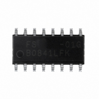
FS6370-01G-XTD ON Semiconductor, FS6370-01G-XTD Datasheet - Page 5

FS6370-01G-XTD
Manufacturer Part Number
FS6370-01G-XTD
Description
IC CLOCK GEN 3-PLL EEPROM 16SOIC
Manufacturer
ON Semiconductor
Type
PLL Clock Generatorr
Datasheet
1.FS6370-01G-XTD.pdf
(28 pages)
Specifications of FS6370-01G-XTD
Pll
Yes
Input
Crystal
Output
CMOS
Number Of Circuits
1
Ratio - Input:output
1:4
Differential - Input:output
No/No
Frequency - Max
230MHz
Divider/multiplier
Yes/No
Voltage - Supply
3 V ~ 5.5 V
Operating Temperature
0°C ~ 70°C
Mounting Type
Surface Mount
Package / Case
16-SOIC (3.9mm Width)
Frequency-max
230MHz
Mounting Style
SMD/SMT
Max Input Freq
230 MHz
Max Output Freq
27 MHz
Number Of Outputs
1
Operating Supply Voltage
5 V to 3.3 V
Operating Temperature Range
0 C to + 70 C
Supply Current
43 mA
Lead Free Status / RoHS Status
Lead free / RoHS Compliant
Other names
766-1025
Available stocks
Company
Part Number
Manufacturer
Quantity
Price
Company:
Part Number:
FS6370-01G-XTD
Manufacturer:
ON Semiconductor
Quantity:
38
FS6370
3.3 Post Dividers
A post divider performs several useful functions. First, it allows the VCO to be operated in a narrower range of speeds compared to the
variety of output clock speeds that the device is required to generate. Second, it changes the basic PLL equation to:
where NP is the post divider modulus. The extra integer in the denominator permits more flexibility in the programming of the loop for
many applications where frequencies must be achieved exactly.
The modulus on two of the four post dividers (post dividers C and D in Figure 2) can be altered without reprogramming by a logic level
on the SEL_CD pin.
4.0 Device Operation
The FS6370 has two modes of operation:
• Program mode: during which either the EEPROM or the FS6370 control registers can be programmed directly with the desired PLL
• Run mode: where the PLL settings stored the EEPROM are transferred to the FS6370 control registers on power-up, and the device
Note that the EEPROM locations are not physically the same registers used to control the FS6370.
Direct access to either the EEPROM or the FS6370 control registers is achieved in program mode. The EEPROM register contents are
automatically transferred to the FS6370 control registers in normal device operation (run mode).
4.1 MODE Pin
The MODE pin controls the mode of operation. A logic-low places the FS6370 in program mode. A logic-high puts the device in run
mode. A pull-up on this pin defaults the device into run mode.
Reprogramming of either the control registers or the EEPROM is permitted at any time if the MODE pin is a logic-low.
Note, however, that a logic-high state on the MODE pin is latched so that only one transfer of EEPROM data to the FS6370 control
registers can occur. If a second transfer of EEPROM data into the FS6370 is desired, power (VDD) must be removed and reapplied to
the device.
The MODE pin also controls the function of the PD/SCL and OE/SDA pins. In run mode, these two pins function as power-down (PD)
and output enable (OE) controls. In program mode, the pins function as the I
4.2 SEL_CD Pin
The SEL_CD pin provides a way to alter the operation of PLL C, muxes C and D, and post dividers C and D without having to
reprogram the device. A logic-low on the SEL_CD pin selects the control bits with a "C1" or "D1" notation, per Table 3. A logic-high on
the SEL_CD pin selects the control bits with "C2" or "D2" notation, per Table 3.
Note that changing between two running frequencies using the SEL_CD pin may produce glitches in the output, especially if the post-
divider(s) is/are altered.
4.3 Oscillator Overdrive
For applications where an external reference clock is provided (and the crystal oscillator is not required), the reference clock should be
connected to XOUT and XIN must be left unconnected (float).
settings
then operates based on those settings
Rev. 3 | Page 5 of 28 | www.onsemi.com
2
C interface for clock (SCL) and data (SDA).


