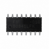
FS6370-01G-XTD ON Semiconductor, FS6370-01G-XTD Datasheet - Page 6

FS6370-01G-XTD
Manufacturer Part Number
FS6370-01G-XTD
Description
IC CLOCK GEN 3-PLL EEPROM 16SOIC
Manufacturer
ON Semiconductor
Type
PLL Clock Generatorr
Datasheet
1.FS6370-01G-XTD.pdf
(28 pages)
Specifications of FS6370-01G-XTD
Pll
Yes
Input
Crystal
Output
CMOS
Number Of Circuits
1
Ratio - Input:output
1:4
Differential - Input:output
No/No
Frequency - Max
230MHz
Divider/multiplier
Yes/No
Voltage - Supply
3 V ~ 5.5 V
Operating Temperature
0°C ~ 70°C
Mounting Type
Surface Mount
Package / Case
16-SOIC (3.9mm Width)
Frequency-max
230MHz
Mounting Style
SMD/SMT
Max Input Freq
230 MHz
Max Output Freq
27 MHz
Number Of Outputs
1
Operating Supply Voltage
5 V to 3.3 V
Operating Temperature Range
0 C to + 70 C
Supply Current
43 mA
Lead Free Status / RoHS Status
Lead free / RoHS Compliant
Other names
766-1025
Available stocks
Company
Part Number
Manufacturer
Quantity
Price
Company:
Part Number:
FS6370-01G-XTD
Manufacturer:
ON Semiconductor
Quantity:
38
FS6370
For best results, make sure the reference clock signal is as jitter-free as possible, can drive a 40 pF load with fast rise and fall times,
and can swing rail-to-rail.
If the reference clock is not a rail-to-rail signal, the reference must be AC coupled to XOUT through a 0.01 µF or 0.1 µF capacitor. A
minimum 1 V peak-to-peak signal is required to drive the internal differential oscillator buffer.
5.0 Run Mode
If the MODE pin is set to a logic-high, the device enters the run mode. The high state is latched (see MODE pin). The FS6370 then
copies the stored EEPROM data into its control registers and begins normal operation based on that data when the self-load is
complete.
The self-load process takes about 89,000 clocks of the crystal oscillator. During the self-load time, all clock outputs are held low. At a
reference frequency of 27 MHz, the self-load takes about 3.3ms to complete.
If the EEPROM is empty (all zeros), the crystal reference frequency provides the clock for all four outputs.
No external programming access to the FS6370 is possible in run mode. The dual-function PD/SCL and OE/SDA pins become a
power-down (PD) and output enable (OE) control, respectively.
5.1 Power-Down and Output Enable
A logic-high on the PD/SCL pin powers down only those portions of the FS6370 which have their respective power-down control bits
enabled. Note that the PD/SCL pin has an internal pull-up.
When a post divider is powered down, the associated output driver is forced low. When all PLLs and post dividers are powered down
the crystal oscillator is also powered down. The XIN pin is forced low, and the XOUT pin is pulled high.
A logic-low on the OE/SDA pin tristates all output clocks. Note that this pin has an internal pull-up.
6.0 Program Mode
If the MODE pin is logic-low, the device enters the program mode. All internal registers are cleared to zero, delivering the crystal
frequency to all outputs. The device allows programming of either the internal 128-bit EEPROM or the on-chip control registers via I
control over the PD/SCL and OE/SDA pins. The EEPROM and the FS6370 act as two separate parallel devices on the same on-chip
I
The dual-function PD/SCL and OE/SDA pins become the serial data I/O (SDA) and serial clock input (SCL) for normal I
communications. Note that power-down and output enable control via the PD/SCL and OE/SDA pins is not available.
6.1 EEPROM Programming
Data must be loaded into the EEPROM in a most-significant-bit (MSB) to least-significant-bit (LSB) order. The register map of the
EEPROM is noted in Table 3.
The device address of the EEPROM is:
6.1.1. Write Operation
The EEPROM can only be written to with the random register write procedure (see Section 8.2.2). The procedure consists of the device
address, the register address, a R/W bit, and one byte of data.
Following the STOP condition, the EEPROM initiates its internally timed 4ms write cycle, and commits the data byte to memory. No
acknowledge signals are generated during the EEPROM internal write cycle.
2
C-bus. Choosing either the EEPROM or the device control registers is done via the I
A6
1
A5
0
A4
1
Rev. 3 | Page 6 of 28 | www.onsemi.com
A3
0
A2
2
X
C device address.
A1
X
A0
X
2
2
C
C


