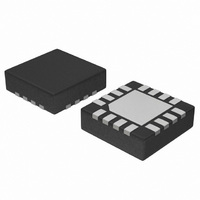
NB6N239SMNG ON Semiconductor, NB6N239SMNG Datasheet - Page 2

NB6N239SMNG
Manufacturer Part Number
NB6N239SMNG
Description
IC CLOCK DIVIDER 3.3V 16-QFN
Manufacturer
ON Semiconductor
Series
ECLinPS MAX™r
Type
Clock Dividerr
Datasheet
1.NB6N239SMNG.pdf
(12 pages)
Specifications of NB6N239SMNG
Pll
No
Input
CML, HSTL, LVDS, LVPECL
Output
LVDS
Number Of Circuits
1
Ratio - Input:output
1:2
Differential - Input:output
Yes/Yes
Frequency - Max
3GHz
Divider/multiplier
Yes/No
Voltage - Supply
3 V ~ 3.465 V
Operating Temperature
-40°C ~ 85°C
Mounting Type
Surface Mount
Package / Case
16-TFQFN Exposed Pad
Frequency-max
3GHz
Function
Clock Divider
Operating Temperature (max)
85C
Operating Temperature (min)
-40C
Package Type
QFN EP
Pin Count
16
Mounting
Surface Mount
Lead Free Status / RoHS Status
Lead free / RoHS Compliant
Other names
NB6N239SMNG
NB6N239SMNGOS
NB6N239SMNGOS
Available stocks
Company
Part Number
Manufacturer
Quantity
Price
Company:
Part Number:
NB6N239SMNG
Manufacturer:
ON Semiconductor
Quantity:
3
*Pins will default LOW when left OPEN.
**Pins will default HIGH when left OPEN.
Table 1. PIN DESCRIPTION
Pin
10
11
12
13
14
15
16
1
2
3
4
5
6
7
8
9
SELB0*
SELB1*
SELA1*
SELA0*
V
Name
MR**
GND
CLK
CLK
EN*
V
BBAC
QB
QB
QA
QA
VT
EP
CC
LVCMOS/LVTTL Input
LVCMOS/LVTTL Input
LVCMOS/LVTTL Input
LVCMOS/LVTTL Input
LVCMOS/LVTTL Input
LVCMOS/LVTTL Input
LVDS, LVPECL, CML,
LVDS, LVPECL, CML,
Power Supply (OPT)
Power Supply
Power Supply
LVDS Output
LVDS Output
LVDS Output
LVDS Output
HSTL Input
HSTL Input
I/O
V
BBAC
CLK
CLK
VT
Figure 2. Pinout: QFN−16 (Top View)
1
2
3
4
Internal 100 W Center−Tapped Termination Pin for CLK and CLK.
Noninverted Differential CLOCK Input.
Inverted Differential CLOCK Input.
Output Voltage Reference for Capacitor Coupled Inputs, only.
Synchronous Output Enable
Clock Divide Select Pin
Clock Divide Select Pin
Negative Supply Voltage
Inverted Differential Output. Typically terminated with 100 W across differential
outputs.
Noninverted Differential Output. Typically terminated with 100 W across differential
outputs.
Inverted Differential Output. Typically terminated with 100 W across differential
outputs.
Noninverted Differential Output. Typically terminated with 100 W across differential
outputs.
Positive Supply Voltage.
Clock Divide Select Pin
Clock Divide Select Pin
Master Reset Asynchronous, Default Open High, Asserted LOW
The Exposed Pad on the QFN−16 package bottom is thermally connected to the die
for improved heat transfer out of package. The pad is not electrically connected to the
die, but is recommended to be electrically and thermally connected to GND on the
PC board.
EN
MR
16
http://onsemi.com
5
SELB0
SELA0
NB6N239S
15
6
2
SELB1
SELA1
14
7
13
V
8
GND
CC
Exposed Pad (EP)
12
10
11
9
Description
QA
QA
QB
QB


