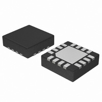
NB6N239SMNG ON Semiconductor, NB6N239SMNG Datasheet - Page 6

NB6N239SMNG
Manufacturer Part Number
NB6N239SMNG
Description
IC CLOCK DIVIDER 3.3V 16-QFN
Manufacturer
ON Semiconductor
Series
ECLinPS MAX™r
Type
Clock Dividerr
Datasheet
1.NB6N239SMNG.pdf
(12 pages)
Specifications of NB6N239SMNG
Pll
No
Input
CML, HSTL, LVDS, LVPECL
Output
LVDS
Number Of Circuits
1
Ratio - Input:output
1:2
Differential - Input:output
Yes/Yes
Frequency - Max
3GHz
Divider/multiplier
Yes/No
Voltage - Supply
3 V ~ 3.465 V
Operating Temperature
-40°C ~ 85°C
Mounting Type
Surface Mount
Package / Case
16-TFQFN Exposed Pad
Frequency-max
3GHz
Function
Clock Divider
Operating Temperature (max)
85C
Operating Temperature (min)
-40C
Package Type
QFN EP
Pin Count
16
Mounting
Surface Mount
Lead Free Status / RoHS Status
Lead free / RoHS Compliant
Other names
NB6N239SMNG
NB6N239SMNGOS
NB6N239SMNGOS
Available stocks
Company
Part Number
Manufacturer
Quantity
Price
Company:
Part Number:
NB6N239SMNG
Manufacturer:
ON Semiconductor
Quantity:
3
NOTE: Device will meet the specifications after thermal equilibrium has been established when mounted in a test socket or printed circuit
Table 8. DC CHARACTERISTICS, LVTTL/LVCMOS INPUTS
Table 9. AC CHARACTERISTICS
NOTE: Device will meet the specifications after thermal equilibrium has been established when mounted in a test socket or printed circuit
7. Measured using a 750 mV, 50% duty cycle clock source. All loading with 100 W across LVDS outputs.
8. Skew is measured between outputs under identical transitions and conditions. Duty cycle skew is defined only for differential operation
9. Input and output voltage swing is a single−ended measurement operating in differential mode.
10. Output Voltage Amplitude (V
Symbol
Symbol
V
V
I
I
f
V
t
t
t
t
t
t
t
t
V
t
t
IH
IL
inMAX
PLH
PHL
RR
s
h
skew
PW
JITTER
r
f
IH
IL
OUTPP
INPP
when the delays are measured from the cross point of the inputs to the cross point of the outputs.
divided by n, f
,
board with maintained transverse airflow greater than 500 lfpm. Electrical parameters are guaranteed only over the declared
operating temperature range. Functional operation of the device exceeding these conditions is not implied. Device specification limit
values are applied individually under normal operating conditions and not valid simultaneously.
board with maintained transverse airflow greater than 500 lfpm. Electrical parameters are guaranteed only over the declared
operating temperature range. Functional operation of the device exceeding these conditions is not implied. Device specification
limit values are applied individually under normal operating conditions and not valid simultaneously.
Input HIGH Voltage (LVCMOS/LVTTL)
Input LOW Voltage (LVCMOS/LVTTL)
Input HIGH Current
Input LOW Current
Maximum Input CLOCK Frequency
Output Voltage Amplitude (Notes 9, 10)
QA(B2, 4, 8), QB(Bn)
QA(B1), QB(Bn)
Propagation Delay to
Output Differential @ 50 MHz
Reset Recovery
Setup Time @ 50 MHz
Hold Time @ 50 MHz
Within−Device Skew @ 50 MHz
Device−to−Device Skew
Duty Cycle Skew
Minimum Pulse Width
RMS Random Clock Jitter
Input Voltage Swing (Differential Configuration)
(Note 9)
Output Rise/Fall Times @ 50 MHz
(20% − 80%)
out
= f
in
B n. Input CLOCK frequency is v3.0 GHz.
Characteristic
QA/QB = (B2, B4, B8, B16)
OHCLK
Characteristic
− V
V
CC
OLCLK
= 3.0 V to 3.465 V; GND = 0 V (Note 7)
f
f
SELA/B, CLK
CLK, SELA/B
in
in
) at input CLOCK frequency, f
v 3.0 GHz
v 1.5 GHz
QA = (B1)
EN, CLK
CLK, EN
CLK, Qn
(Note 8)
(Note 8)
(Note 8)
MR, Qn
Qn, Qn
MR
http://onsemi.com
Min
200
200
550
420
150
700
550
100
3.0
1.5
70
0
0
0
6
(V
−300
−40°C
Typ
350
350
−90
−60
200
120
65
25
25
5
CC
= 3.0 V to 3.465 V, GND = 0 V, T
−GND
in
Max
V
450
450
780
660
190
. The output frequency, f
30
80
40
2
CC
GND
−150
−150
Min
2.0
Min
200
200
550
420
150
700
550
100
3.0
1.5
70
0
0
0
−300
Typ
25°C
350
350
−90
−60
200
120
65
30
30
5
Typ
−GND
Max
V
450
450
780
660
190
30
90
45
2
CC
out
, is the input CLOCK frequency
A
= −40°C to +85°C)
Min
200
200
550
420
150
700
550
100
3.0
1.5
70
0
0
0
−300
Max
V
Typ
350
350
−90
−60
200
120
150
150
85°C
0.8
65
30
30
6
CC
−GND
Max
V
450
450
780
660
190
35
90
45
2
CC
Unit
mA
mA
GHz
Unit
V
V
mV
mV
ps
ps
ps
ps
ps
ps
ps
ps


