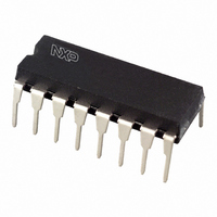
74HCT9046AN,112 NXP Semiconductors, 74HCT9046AN,112 Datasheet - Page 8

74HCT9046AN,112
Manufacturer Part Number
74HCT9046AN,112
Description
IC PLL W/BAND GAP VCO 16-DIP
Manufacturer
NXP Semiconductors
Type
Phase Lock Loop (PLL)r
Series
74HCTr
Datasheet
1.74HCT9046AD118.pdf
(43 pages)
Specifications of 74HCT9046AN,112
Number Of Circuits
1
Package / Case
16-DIP (0.300", 7.62mm)
Pll
Yes
Input
Clock
Output
Clock
Ratio - Input:output
2:2
Differential - Input:output
No/No
Frequency - Max
16MHz
Divider/multiplier
No/No
Voltage - Supply
4.5 V ~ 5.5 V
Operating Temperature
-40°C ~ 125°C
Mounting Type
Through Hole
Frequency-max
16MHz
Supply Voltage (max)
5.5 V
Supply Voltage (min)
4.5 V
Maximum Operating Temperature
+ 125 C
Minimum Operating Temperature
- 40 C
Mounting Style
SMD/SMT
Operating Supply Voltage
4.5 V to 5.5 V
Lead Free Status / RoHS Status
Lead free / RoHS Compliant
Lead Free Status / RoHS Status
Lead free / RoHS Compliant, Lead free / RoHS Compliant
Other names
568-2913-5
935044170112
935044170112
NXP Semiconductors
74HCT9046A_6
Product data sheet
waveforms for the PC1 loop locked at f
actual waveforms across the VCO capacitor at pins C1A and C1B (V
show the relation between these ramps and the VCO_OUT voltage.
The frequency capture range (2f
which the PLL will lock if it was initially out-of-lock. The frequency lock range (2f
defined as the frequency range of the input signals on which the loop will stay locked if it
was initially in lock. The capture range is smaller or equal to the lock range.
With PC1, the capture range depends on the low-pass filter characteristics and can be
made as large as the lock range. This configuration remains locked even with very noisy
input signals. Typical behavior of this type of phase comparator is that it may lock to input
frequencies close to the harmonics of the VCO center frequency.
Fig 6.
Phase comparator 1; average output voltage as a function of input phase
difference
Rev. 06 — 15 September 2009
V
DEM_OUT(AV)
V
DEM _OUT
0.5V
V
CC
CC
0
) is defined as the frequency range of input signals on
0
0
PC_IN
o
=
0
V
are shown in
PCI _OUT
=
SIG_IN
90
=
o
V
---------- -
PLL with band gap controlled VCO
CC
–
Figure
PC_IN
COMP_IN
SIG_IN
mbd101
7. This figure also shows the
74HCT9046A
180
–
o
COMP_IN
C1A
© NXP B.V. 2009. All rights reserved.
and V
C1B
L
) is
) to
8 of 43


