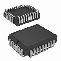
CY7B9911-5JC Cypress Semiconductor Corp, CY7B9911-5JC Datasheet

CY7B9911-5JC
Specifications of CY7B9911-5JC
Available stocks
Related parts for CY7B9911-5JC
CY7B9911-5JC Summary of contents
Page 1
... Document Number: 38-07209 Rev. *F Programmable Skew Clock Buffer Functional Description The CY7B9911 High Speed Programmable Skew Clock Buffer (PSCB) offers user selectable control over system clock functions. This multiple output clock driver provides the system integrator with functions necessary to optimize the timing of high performance computer systems ...
Page 2
... Maximum Ratings............................................................. 5 Operating Range............................................................... 6 Document Number: 38-07209 Rev. *F RoboClock+™ Electrical Characteristics................................................. 6 Capacitance ...................................................................... 7 AC Timing Diagrams ........................................................ 9 Operational Mode Descriptions .................................... 10 Ordering Information...................................................... 13 Package Diagram............................................................ 13 Document History Page ................................................. 14 Sales, Solutions, and Legal Information ...................... 15 Worldwide Sales and Design Support....................... 15 Products .................................................................... 15 PSoC Solutions ......................................................... 15 CY7B9911 Page [+] Feedback ...
Page 3
... Document Number: 38-07209 Rev 3F1 4F0 6 28 4F1 CCQ CY7B9911 CCN 4Q1 10 24 4Q0 23 11 GND 12 22 GND Description Table 2. Table 3. Table 3. Table 3. Table 3. CY7B9911 RoboClock+™ 2F0 GND 1F1 1F0 V CCN 1Q0 1Q1 GND GND Table 3. Table 3 Table 3 Table 3 Page [+] Feedback ...
Page 4
... LOW Approximate MID MID Which t = 1.0 ns MID HIGH U HIGH LOW 22.7 HIGH MID 38.5 HIGH HIGH 62.5 CY7B9911 RoboClock+™ selected. U [1] Output Functions 1Q0, 1Q1, 3Q0, 3Q1 4Q0, 4Q1 3F0, 4F0 2Q0, 2Q1 –4t Divide by 2 Divide –3t –6t – – ...
Page 5
... The TEST input is a three level input. In normal system operation, this pin is connected to ground, enabling the CY7B9911 to operate as explained in the previous section (for testing purposes). Any of the three level inputs can have a removable jumper to ground or be tied LOW through a 100 ...
Page 6
... CY7B9911 must be tested one output at a time, output shorted for less than one second, less than 10% duty cycle. Room temperature only. 7. Total output current per output pair is approximated by the following expression that includes device current plus load current: CY7B9911:ICCN = [(4 + 0.11F) + [((835 – ...
Page 7
... Test conditions assume signal transition times unless otherwise specified. Parameter Description C Input Capacitance IN 5V R1=130 R1 R2= (Includes fixture and probe capacitance TTL AC Test Load (CY7B9911) Document Number: 38-07209 Rev. *F Test Conditions MHz 5. Figure 3. AC Test Loads and Waveforms 2.0V V =1.5V th 0.8V 0.0V ...
Page 8
... AC Test Loads and Waveforms . Other outputs are divided or inverted but not shifted. U delay), Inverted (4Q0 and 4Q1 only with 4F0 = 4F1 = HIGH), and Divided (3Qx and 4Qx only in Divide-by within specified limits. PD CY7B9911 RoboClock+™ CY7B9911–7 Max Min Typ Max ...
Page 9
... Figure 4. AC Timing Diagrams t t REF RPWL t RPWH t ODCV t ODCV t t SKEWPR, SKEWPR SKEW0,1 SKEW0,1 t SKEW2 t SKEW3,4 t SKEW3,4 t SKEW1,3, 4 REF L1 4Q0 L2 4Q1 3Q0 3Q1 L3 2Q0 2Q1 1Q0 L4 1Q1 CY7B9911 RoboClock+™ SKEW2 t SKEW3,4 t SKEW2,4 LOAD Z 0 LOAD Z 0 LOAD Z 0 LOAD Z 0 Page [+] Feedback ...
Page 10
... REF. This causes the 1Q, 2Q, and 3Q outputs to become the “inverted” outputs with respect to the REF input. By selecting the output to connect to FB, you can have two inverted and six non-inverted outputs or six inverted and two CY7B9911 RoboClock+™ LOAD Z ...
Page 11
... PSCB performs all of the functions described in this section at the same time. It can multiply by two and four or divide by two (and four) at the same time that it is shifting its outputs over a wide range or maintaining zero skew between selected outputs. CY7B9911 RoboClock+™ REF 10 MHz ...
Page 12
... TEST Figure 10 shows the CY7B9911 connected in series to construct a zero-skew clock distribution tree between boards. Delays of the downstream clock buffers are programmed to compensate for the wire length (that is, select negative skew equal to the wire delay) necessary to connect them to the master clock source, Document Number: 38-07209 Rev ...
Page 13
... Plastic Leaded Chip Carrier - Tape and Reel T = Tape and Reel, Blank = Standard Temperature Range C = Commercial = 0 ° °C Package Type Plastic Leaded Chip Carrier Propagation delay 500 ps max Base part number Company ID Cypress CY7B9911 RoboClock+™ Operating Range Commercial Commercial 51-85002 *C Page ...
Page 14
... Document History Page Document Title: CY7B9911 RoboClock+™ Programmable Skew Clock Buffer Document Number: 38-07209 Orig. of Revision ECN Change ** 110342 SZV *A 1199925 KVM/AESA *B 1286064 AESA *C 2593494 CXQ/PYRS *D 2761988 CXQ *E 2894070 CXQ *F 3076920 CXQ Document Number: 38-07209 Rev. *F Submission Description of Change Date ...
Page 15
... Semiconductor Corporation. All products and company names mentioned in this document may be the trademarks of their respective holders. cypress.com/go/plc Revised November 02, 2010 2 C components from Cypress or one of its sublicensed Associated Companies conveys a license under the 2 C Standard Specification as defined by Philips. RoboClock trademark of Cypress CY7B9911 RoboClock+™ PSoC Solutions psoc.cypress.com/solutions PSoC 1 | PSoC 3 ...


