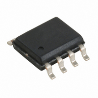
CY2304SXC-1 Cypress Semiconductor Corp, CY2304SXC-1 Datasheet

CY2304SXC-1
Specifications of CY2304SXC-1
CY2304SXC-1
Available stocks
Related parts for CY2304SXC-1
CY2304SXC-1 Summary of contents
Page 1
... CY2304-1 Bank CY2304-2 Bank A CY2304-2 Bank B Cypress Semiconductor Corporation Document Number: 38-07247 Rev. *J 3.3 V Zero Delay Buffer one of the outputs. The input-to-output skew is guaranteed to be less than 250 ps, and output-to-output skew is guaranteed to be less than 200 ps. The CY2304 has two banks of two outputs each. ...
Page 2
... Zero Delay and Skew Control .......................................... 4 Maximum Ratings ............................................................. 5 Operating Conditions for CY2304SXC Commercial Temperature Devices ....................................................... 5 Electrical Characteristics for CY2304SXC Commercial Temperature Devices ....................................................... 5 Switching Characteristics for CY2304SXC Commercial Temperature Devices ....................................................... 6 Electrical Characteristics for CY2304SXI Industrial Temperature Devices ....................................................... 7 Operating Conditions for CY2304SXI Industrial Temperature Devices ....................................................... 7 Document Number: 38-07247 Rev ...
Page 3
Pinout l Table 2. Pin Definitions - 8-pin SOIC Pin Signal [1] 1 REF 2 CLKA1 3 CLKA2 4 GND 5 CLKB1 6 CLKB2 FBK Notes 1. Weak pull-down. 2. Weak pull-down on all outputs. Document ...
Page 4
Zero Delay and Skew Control Figure 2. REF. Input to CLKA/CLKB Delay vs. Difference in Loading Between FBK Pin and CLKA/CLKB Pins To close the feedback loop of the CY2304, the FBK pin can be driven from any of the ...
Page 5
... Load capacitance (below 100 MHz) L Load capacitance (from 100 MHz to 133 MHz) C [3] Input capacitance IN t Power-up time for all (power ramps must be monotonic) Electrical Characteristics for CY2304SXC Commercial Temperature Devices Parameter Description V Input LOW voltage IL V Input HIGH voltage IH I Input LOW current IL ...
Page 6
... Switching Characteristics for CY2304SXC Commercial Temperature Devices [5] Name Parameter t Output frequency 1 t Output frequency 1 t [6] t Duty cycle = (–1,–2) t [6] t Duty cycle = (–2) t [6] t Duty cycle = (–1,–2) t [6] Rise time 3 (–1, –2) [6] t Rise time 3 (– ...
Page 7
Operating Conditions for CY2304SXI Industrial Temperature Devices Parameter V Supply voltage DD T Operating temperature (ambient temperature Load capacitance (below 100 MHz) L Load capacitance (from 100 MHz to 133 MHz) C Input capacitance IN Electrical Characteristics for ...
Page 8
Switching Characteristics for CY2304SXI Industrial Temperature Devices [8] Parameter Name t Output frequency 1 t Output frequency 1 t [9] t Duty cycle = (–1,–2) t [9] t Duty cycle = (–2) ...
Page 9
Switching Waveforms OUTPUT OUTPUT OUTPUT INPUT FBK FBK, Device 1 FBK, Device 2 Document Number: 38-07247 Rev. *J Figure 2. Duty Cycle Timing 1.4 V 1.4 V 1.4 V Figure 3. All Outputs Rise/Fall Time 2.0 ...
Page 10
Document Number: 38-07247 Rev. *J Figure 7. Test Circuit # CLK OUTPUTS C LOAD V DD GND GND Test circuit for all parameters CY2304 OUT Page [+] Feedback ...
Page 11
... SOIC CY2304SXI–1 8-pin 150-mil SOIC - Tape and Reel CY2304SXI–1T 8-pin 150-mil SOIC CY2304SXC–2 8-pin 150-mil SOIC - Tape and Reel CY2304SXC–2T 8-pin 150-mil SOIC CY2304SXI–2 8-pin 150-mil SOIC - Tape and Reel CY2304SXI–2T Ordering Code Definitions CY ...
Page 12
Package Drawing and Dimensions Document Number: 38-07247 Rev. *J Figure 8. 8-pin (150-Mil) SOIC S8 CY2304 51-85066 *D Page [+] Feedback ...
Page 13
Acronyms Acronym Description PCI Personal computer interconnect PLL Phase locked loop SDRAM Synchronous dynamic random access memory SOIC Small outline integrated circuit TSSOP Thin small outline package ZDB Zero delay buffer Document Number: 38-07247 Rev. *J Document Conventions Units of ...
Page 14
... Removed parts CY2304SC-1, CY2304SC-1T,CY2304SC-2,CY2304SC-2T,CY2304SI-1,CY2304SI-1T from the ordering information table. Updated Package Diagram. 10/27/2010 Corrected part number in all table titles (pages from CY2304SC-X and CY2304SI-X to CY2304SXC and CY2304SXI. Removed “except t ” from Figure 7 8 02/04/2011 Updated in new template. 03/24/2011 Added duty cycle spec for 83.0 MHz output condition. ...
Page 15
... Cypress against all charges. Any Source Code (software and/or firmware) is owned by Cypress Semiconductor Corporation (Cypress) and is protected by and subject to worldwide patent protection (United States and foreign), United States copyright laws and international treaty provisions. Cypress hereby grants to licensee a personal, non-exclusive, non-transferable license to copy, use, modify, create derivative works of, and compile the Cypress Source Code and derivative works for the sole purpose of creating custom software and or firmware in support of licensee product to be used only in conjunction with a Cypress integrated circuit as specified in the applicable agreement ...


