CY2304SXC-1 Cypress Semiconductor Corp, CY2304SXC-1 Datasheet - Page 8
CY2304SXC-1
Manufacturer Part Number
CY2304SXC-1
Description
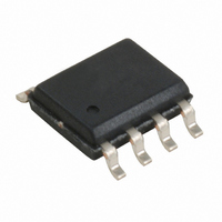
IC CLK ZDB 4OUT 133MHZ 8SOIC
Manufacturer
Cypress Semiconductor Corp
Type
Fanout Distribution, Zero Delay Bufferr
Datasheet
1.CY2304SXC-2.pdf
(15 pages)
Specifications of CY2304SXC-1
Number Of Circuits
1
Package / Case
8-SOIC (3.9mm Width)
Pll
Yes
Input
Clock
Output
Clock
Ratio - Input:output
1:4
Differential - Input:output
No/No
Frequency - Max
133.3MHz
Divider/multiplier
No/No
Voltage - Supply
3 V ~ 3.6 V
Operating Temperature
0°C ~ 70°C
Mounting Type
Surface Mount
Frequency-max
133MHz
Output Frequency Range
10 MHz to 133.3 MHz
Supply Voltage (max)
3.6 V
Supply Voltage (min)
3 V
Maximum Operating Temperature
+ 70 C
Minimum Operating Temperature
0 C
Mounting Style
SMD/SMT
Operating Supply Voltage
3.3 V
Number Of Elements
1
Supply Current
45mA
Operating Supply Voltage (typ)
3.3V
Operating Temp Range
0C to 70C
Package Type
SOIC
Operating Supply Voltage (min)
3V
Operating Supply Voltage (max)
3.6V
Operating Temperature Classification
Commercial
Pin Count
8
Lead Free Status / RoHS Status
Lead free / RoHS Compliant
Lead Free Status / RoHS Status
Lead free / RoHS Compliant, Lead free / RoHS Compliant
Other names
428-2192-5
CY2304SXC-1
CY2304SXC-1
Available stocks
Company
Part Number
Manufacturer
Quantity
Price

Company:
Part Number:
CY2304SXC-1T
Manufacturer:
CY
Quantity:
158
Part Number:
CY2304SXC-1T
Manufacturer:
CYPRESS/赛普拉斯
Quantity:
20 000


Document Number: 38-07247 Rev. *J
Notes
Switching Characteristics for CY2304SXI Industrial Temperature Devices
t
t
t
t
t
t
t
t
t
t
t
t
t
t
t
8. All parameters are specified with loaded output.
9. Parameter is guaranteed by design and characterization. Not 100% tested in production.
1
1
DC
DC
DC
3
3
4
4
5
6
7
J
J
LOCK
Parameter
[8]
Output frequency
Output frequency
Duty cycle
(–1,–2)
Duty cycle
(–2)
Duty cycle
(–1,–2)
Rise time
(–1, –2)
Rise time
(–1, –2)
Fall time
(–1, –2)
Fall time
(–1, –2)
Output-to-output skew on
same bank (–1,–2)
Output bank A to output
bank B skew (–1)
Output bank A to output
bank B skew (–2)
Skew, REF rising edge to
FBK rising edge
Device-to-device skew
Cycle-to-cycle jitter
(–1)
Cycle-to-cycle jitter
(–2)
PLL lock time
[9]
[9]
[9]
[9]
[9]
[9]
[9]
Name
= t
= t
= t
[9]
2
2
2
[9]
t
t
t
[9]
[9]
[9]
1
1
1
[9]
30-pF load, All devices
15-pF load, All devices
Measured at 1.4 V, F
30-pF load
Measured at 1.4 V,
F
Measured at 1.4 V, F
15-pF load
Measured between 0.8 V and 2.0 V,
30-pF load
Measured between 0.8 V and 2.0 V,
15-pF load
Measured between 0.8 V and 2.0 V,
30-pF load
Measured between 0.8 V and 2.0 V,
15-pF load
All outputs equally loaded
All outputs equally loaded
All outputs equally loaded
Measured at V
Measured at V
devices
Measured at 66.67 MHz, loaded outputs,
15-pF load
Measured at 66.67 MHz, loaded outputs,
30-pF load
Measured at 133.3 MHz, loaded outputs,
15-pF load
Measured at 66.67 MHz, loaded outputs,
30-pF load
Measured at 66.67 MHz, loaded outputs,
15-pF load
Stable power supply, valid clocks
presented on REF and FBK pins
OUT
= 83.0 MHz, 15-pF load
Test Conditions
DD
DD
/2
/2 on the FBK pins of
OUT
OUT
= 66.66 MHz,
< 50 MHz,
40.0
40.0
45.0
Min
10
10
–
–
–
–
–
–
–
–
–
–
–
–
–
–
–
50.0
50.0
50.0
Typ
–
–
–
–
–
–
–
–
–
0
0
–
–
–
–
–
–
133.3
250
Max
60.0
60.0
55.0
2.50
1.50
2.50
1.50
100
200
200
400
500
180
200
100
400
380
1.0
CY2304
Page 8 of 15
MHz
MHz
Unit
ms
ns
ns
ns
ns
ps
ps
ps
ps
ps
ps
ps
ps
ps
ps
%
%
%
[+] Feedback
Related parts for CY2304SXC-1
Image
Part Number
Description
Manufacturer
Datasheet
Request
R

Part Number:
Description:
Manufacturer:
Cypress Semiconductor Corp
Datasheet:
Part Number:
Description:
Manufacturer:
Cypress Semiconductor Corp
Datasheet:
Part Number:
Description:
Manufacturer:
Cypress Semiconductor Corp
Datasheet:
Part Number:
Description:
Manufacturer:
Cypress Semiconductor Corp
Datasheet:
Part Number:
Description:
Manufacturer:
Cypress Semiconductor Corp
Datasheet: