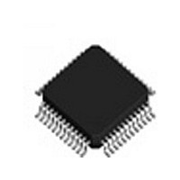
MPC9600AE IDT, Integrated Device Technology Inc, MPC9600AE Datasheet - Page 12

MPC9600AE
Manufacturer Part Number
MPC9600AE
Description
IC PLL CLK DRIVER LV 48-LQFP
Manufacturer
IDT, Integrated Device Technology Inc
Type
PLL Clock Driverr
Datasheet
1.MPC9600AER2.pdf
(14 pages)
Specifications of MPC9600AE
Pll
Yes with Bypass
Input
LVCMOS, LVPECL
Output
LVCMOS
Number Of Circuits
1
Ratio - Input:output
2:22
Differential - Input:output
Yes/No
Frequency - Max
200MHz
Divider/multiplier
Yes/No
Voltage - Supply
2.375 V ~ 3.465 V
Operating Temperature
-40°C ~ 85°C
Mounting Type
Surface Mount
Package / Case
48-LQFP
Frequency-max
200MHz
Number Of Elements
1
Supply Current
5mA
Pll Input Freq (min)
16.67MHz
Pll Input Freq (max)
50MHz
Operating Supply Voltage (typ)
2.5/3.3V
Operating Temp Range
-40C to 85C
Package Type
TQFP
Output Frequency Range
50 to 200MHz
Operating Supply Voltage (min)
2.375V
Operating Supply Voltage (max)
3.465V
Operating Temperature Classification
Industrial
Pin Count
48
Lead Free Status / RoHS Status
Lead free / RoHS Compliant
Available stocks
Company
Part Number
Manufacturer
Quantity
Price
Company:
Part Number:
MPC9600AE
Manufacturer:
IDT, Integrated Device Technology Inc
Quantity:
10 000
Company:
Part Number:
MPC9600AER2
Manufacturer:
IDT
Quantity:
1 186
Company:
Part Number:
MPC9600AER2
Manufacturer:
Sigmatel
Quantity:
77
Company:
Part Number:
MPC9600AER2
Manufacturer:
IDT, Integrated Device Technology Inc
Quantity:
10 000
Part Number:
MPC9600AER2
Manufacturer:
FESSCALE
Quantity:
20 000
IDT™ / ICS™ 2.5V AND 3.3V LVCMOS PLL CLOCK DRIVER
Figure 14. Propagation Delay (t
The variation in cycle time of a signal between adjacent cycles, over a random
sample of adjacent cycle pairs
MPC9600
LOW VOLTAGE, 2.5V AND 3.3V LVCMOS PLL CLOCK DRIVER
PCLK
PCLK
FB_IN
The time from the PLL controlled edge to the non controlled edge, divided
by the time between PLL controlled edges, expressed as a percentage
(PCLK)
FB_IN
CCLK
The deviation in T
mean in a random sample of cycles
Figure 16. Output Duty Cycle (DC)
Figure 18. Cycle-to-Cycle Jitter
T
N
t
P
0
Figure 20. I/O Jitter
t
for a controlled edge with respect to a T
(∅)
Test Reference
T
N+1
T
0
DC = t
P
V
/T
PP
T
0
Ø
T
JIT(CC)
x 100%
JIT(∅)
, status phase offset)
= |T
= |T
0
N
–T
–T
1
N+1
mean|
V
V
GND
CC
CC
|
0
÷ 2
V
V
V
GND
CC
CC
CMR
÷ 2
12
The pin-to-pin skew is defined as the worst case difference in propagation delay
between any similar delay path within a single device
Figure 15. Propagation Delay (t
FB_IN
The deviation in cycle time of a signal with respect to the ideal period
over a random sample of cycles
t
F
TCLK
Figure 21. Transition Time Test Reference
Figure 17. Output-to-Output Skew t
T
0
Figure 19. Period Jitter
t
(∅)
t
t
R
SK(O)
MPC9600 REV. 5 NOVEMBER 10, 2008
V
T
CC
JIT(P)
Ø
0.55
2.4
= 3.3 V
) Test Reference
= |T
N
–1/f
SK(O)
0
|
V
CC
V
V
GND
V
V
GND
V
V
GND
V
V
GND
CC
CC
CC
CC
1.8
= 2.5 V
0.6
CC
CC
CC
CC
÷ 2
÷ 2
÷ 2
÷ 2


