IDT5V49EE702NDGI8 IDT, Integrated Device Technology Inc, IDT5V49EE702NDGI8 Datasheet - Page 14
IDT5V49EE702NDGI8
Manufacturer Part Number
IDT5V49EE702NDGI8
Description
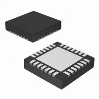
IC PLL CLK GEN 200MHZ 28VQFN
Manufacturer
IDT, Integrated Device Technology Inc
Type
Clock Generator, Multiplexerr
Datasheet
1.IDT5V49EE702NDGI8.pdf
(34 pages)
Specifications of IDT5V49EE702NDGI8
Pll
Yes with Bypass
Input
LVCMOS, LVTTL, Crystal
Output
HCSL, LVCMOS, LVDS, LVPECL, LVTTL
Number Of Circuits
1
Ratio - Input:output
2:7
Differential - Input:output
No/Yes
Frequency - Max
500MHz
Divider/multiplier
Yes/Yes
Voltage - Supply
3.135 V ~ 3.465 V
Operating Temperature
-40°C ~ 85°C
Mounting Type
Surface Mount
Package / Case
28-VQFN Exposed Pad, 28-HVQFN, 28-SQFN, 28-DHVQFN
Frequency-max
500MHz
Lead Free Status / RoHS Status
Lead free / RoHS Compliant
Other names
IDT5V49EE702DLGI8
IDT5V49EE702DLGI8
IDT5V49EE702DLGI8


Progread
Note: If the expected read command is not from the next higher register to the previous read or write command, then set a
known “read” register address prior to a read operation by issuing the following command:
Prior to Progread Command Set Register Address
The user can ignore the STOP condition above and use a repeated START condition instead, straight after the slave
acknowledgement bit (i.e., followed by the Progread command):
Progsave
Note:
PROGWRITE is for writing to the IDT5V49EE702 registers.
PROGREAD is for reading the IDT5V49EE702 registers.
PROGSAVE is for saving all the contents of the IDT5V49EE702 registers to the EEPROM.
PROGRESTORE is for loading the entire EEPROM contents to the IDT5V49EE702 registers.
Progrestore
EEPROM Interface
The IDT5V49EE702 can also store its configuration in an internal EEPROM. The contents of the device's internal
programming registers can be saved to the EEPROM by issuing a save instruction (ProgSave) and can be loaded back to
the internal programming registers by issuing a restore instruction (ProgRestore).
To initiate a save or restore using I
set to “0”, followed by the appropriate command code. The save or restore instruction executes after the STOP condition is
issued by the Master, during which time the IDT5V49EE702 will not generate Acknowledge bits. The IDT5V49EE702 will
acknowledge the instructions after it has completed execution of them. During that time, the I
as busy by all other users of the bus.
On power-up of the IDT5V49EE702, an automatic restore is performed to load the EEPROM contents into the internal
programming registers. The IDT5V49EE702 will be ready to accept a programming instruction once it acknowledges its 7-bit
I
IDT® EEPROM PROGRAMMABLE CLOCK GENERATOR
2
C address.
S
S
S
S
IDT5V49EE702
EEPROM PROGRAMMABLE CLOCK GENERATOR
Address
Address
Address
Address
7-bits
7-bits
7-bits
7-bits
R/W
R/W
R/W
R/W
1
0
0
0
ACK
1-bit
ACK
ACK
ACK
1-bit
1-bit
1-bit
ID Byte
2
8-bits
Command Code
Command Code
Command Code
8-bits: xxxx xx00
8-bits: xxxx xx01
8-bits: xxxx xx10
C, only two bytes are transferred. The Device Address is issued with the read/write bit
ACK
1-bit
Progread Command Frame
Data_1
8-bits
ACK
ACK
ACK
1-bit
1-bit
1-bit
14
ACK
1-bit
Register
P
P
8-bits
Data_2
8-bits
ACK
1-bit
ACK
1-bit
P
Data_last NACK
8-bits
2
C bus should be interpreted
IDT5V49EE702
CLOCK SYNTHESIZER
1-bit
P
REV F 022310
Related parts for IDT5V49EE702NDGI8
Image
Part Number
Description
Manufacturer
Datasheet
Request
R

Part Number:
Description:
TRANSLATION DEVICE DPI 80-PQFP
Manufacturer:
IDT, Integrated Device Technology Inc
Datasheet:
Part Number:
Description:
IDT PART
Manufacturer:
IDT, Integrated Device Technology Inc
Datasheet:
Part Number:
Description:
IC LIU T1/E1/J1 OCTAL 256PBGA
Manufacturer:
IDT, Integrated Device Technology Inc
Datasheet:

Part Number:
Description:
IC FREQ TIMING GENERATOR 28TSSOP
Manufacturer:
IDT, Integrated Device Technology Inc
Datasheet:
Part Number:
Description:
IC CLK DVR PLL 1:10 40VFQFPN
Manufacturer:
IDT, Integrated Device Technology Inc
Datasheet:
Part Number:
Description:
IC CLK FANOUT BUFFER 1:18 32LQFP
Manufacturer:
IDT, Integrated Device Technology Inc
Datasheet:
Part Number:
Description:
IC CLK FANOUT BUFFER 1:18 32LQFP
Manufacturer:
IDT, Integrated Device Technology Inc
Datasheet:
Part Number:
Description:
IC CK505 VREG/RES 56TSSOP
Manufacturer:
IDT, Integrated Device Technology Inc
Datasheet:

Part Number:
Description:
IC SDRAM CLK DVR 1:10 48-TSSOP
Manufacturer:
IDT, Integrated Device Technology Inc
Datasheet:

Part Number:
Description:
IC CLK DVR PLL 1:10 48TSSOP
Manufacturer:
IDT, Integrated Device Technology Inc
Datasheet:
Part Number:
Description:
IC FLEXPC CLK PROGR P4 56-TSSOP
Manufacturer:
IDT, Integrated Device Technology Inc
Datasheet:
Part Number:
Description:
IC FLEXPC CLK PROGR P4 56-TSSOP
Manufacturer:
IDT, Integrated Device Technology Inc
Datasheet:
Part Number:
Description:
IC FLEXPC CLK PROGR P4 56-SSOP
Manufacturer:
IDT, Integrated Device Technology Inc
Datasheet:

Part Number:
Description:
IC PLL CLK DRIVER 2.5V 28-TSSOP
Manufacturer:
IDT, Integrated Device Technology Inc
Datasheet:
Part Number:
Description:
IC CLOCK DRIVER 2.5V 24-TSSOP
Manufacturer:
IDT, Integrated Device Technology Inc
Datasheet: