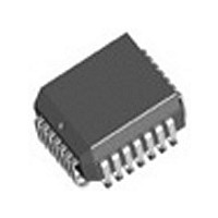
IDT74FCT388915TDJG8 IDT, Integrated Device Technology Inc, IDT74FCT388915TDJG8 Datasheet - Page 7

IDT74FCT388915TDJG8
Manufacturer Part Number
IDT74FCT388915TDJG8
Description
IC PLL CLK GENERATOR 3ST 28-PLCC
Manufacturer
IDT, Integrated Device Technology Inc
Series
74FCTr
Type
PLL Clock Driverr
Datasheet
1.IDT74FCT388915TBJG8.pdf
(10 pages)
Specifications of IDT74FCT388915TDJG8
Pll
Yes with Bypass
Input
LVTTL
Output
LVCMOS, LVTTL
Number Of Circuits
1
Ratio - Input:output
2:8
Differential - Input:output
No/No
Frequency - Max
133MHz
Divider/multiplier
Yes/Yes
Voltage - Supply
3 V ~ 3.6 V
Operating Temperature
0°C ~ 70°C
Mounting Type
Surface Mount
Package / Case
28-PLCC
Frequency-max
133MHz
Number Of Elements
1
Pll Input Freq (min)
10MHz
Pll Input Freq (max)
133MHz
Operating Supply Voltage (typ)
3.3V
Operating Temp Range
0C to 70C
Package Type
PLCC
Output Frequency Range
10 to 133MHz
Operating Supply Voltage (min)
3V
Operating Supply Voltage (max)
3.6V
Operating Temperature Classification
Commercial
Pin Count
28
Lead Free Status / RoHS Status
Lead free / RoHS Compliant
Other names
74FCT388915TDJG8
Available stocks
Company
Part Number
Manufacturer
Quantity
Price
Company:
Part Number:
IDT74FCT388915TDJG8
Manufacturer:
IDT, Integrated Device Technology Inc
Quantity:
10 000
The frequency relationship shown here is applicable to all Q outputs (Q0, Q1,
Q2, Q3 and Q4).
1:2 INPUT TO "Q" OUTPUT
FREQUENCY RELATIONSHIP
internal PLL will line up the positive edges of Q/2 and SYNC, thus the Q/2
frequency will equal the SYNC frequency. The Q outputs (Q0-Q4, Q5) will
always run at 2X the Q/2 frequency, and the 2Q output will run at 4X the Q/2
frequency.
1:1 INPUT TO "Q" OUTPUT
FREQUENCY RELATIONSHIP
internal PLL will line up the positive edges of Q4 and SYNC, thus the Q4
frequency (and the rest of the "Q" outputs) will equal the SYNC frequency. The
Q/2 output will always run at 1/2 the Q frequency, and the 2Q output will run
at 2X the Q frequency.
12.5 MHz
input
IDT74FCT388915T
3.3V LOW SKEW PLL-BASED CMOS CLOCK DRIVER (3-STATE)
Allowable Input Frequency Range:
10MHz to ( f2Q MAX Spec)/4 (for FREQ_SEL HIGH)
5MHz to (f2Q MAX Spec)/8 (for FREQ_SEL LOW)
Figure 3a. Wiring Diagram and Frequency Relationships With Q/
In this application, the Q/2 output is connected to the FEEDBACK input. The
In this application, the Q4 output is connected to the FEEDBACK input. The
LOW
FEEDBACK
REF_SEL
SYNC(0)
V
GND(AN)
FQ_SEL
LF
OE/
CC
HIGH
HIGH
12.5 M Hz feedback signal
(AN)
RST
2 Output Feedback
Q5
Q0
FCT388915T
Q1
Q4
PLL_EN
HIGH
2Q
50 M Hz signal
Q/2
Q3
Q2
25 MHz
Outputs
Clock
"Q"
7
25 MHz
input
2:1 INPUT TO "Q" OUTPUT
FREQUENCY RELATIONSHIP
internal PLL will line up the positive edges of 2Q and SYNC, thus the 2Q
frequency will equal the SYNC frequency. The Q/2 output will always run at
1/4 the 2Q frequency, and the Q output will run at 1/2 the 2Q frequency.
50 MHz
input
LOW
LOW
Allowable Input Frequency Range:
20MHz to (f2Q MAX Spec)/2 (for FREQ_SEL HIGH)
10MHz to (f2Q MAX Spec)/4 (for FREQ_SEL LOW)
Allowable Input Frequency Range:
40MHz to (f2Q MAX Spec) (for FREQ_SEL HIGH)
20MHz to (f2Q MAX Spec)/2 (for FREQ_SEL LOW)
In this application, the 2Q output is connected to the FEEDBACK input. The
Figure 3b. Wiring Diagram and Frequency Relationships With
Figure 3c. Wiring Diagram and Frequency Relationships With
25 MHz feedback signal
FEEDBACK
REF_SEL
SYNC(0)
V
LF
GND(AN)
FQ_SEL
FEEDBACK
REF_SEL
SYNC(0)
V
GND(AN)
FQ_SEL
LF
50 MHz feedback signal
OE/
OE/
CC
CC
HIGH
HIGH
HIGH
HIGH
(AN)
(AN)
RST
RST
Q5
Q0
Q 0
Q4 Output Feedback
2Q Output Feedback
Q5
FCT388915T
FCT388915T
COMMERCIAL TEMPERATURE RANGE
Q1
Q4
Q1
Q4
PLL_EN
PLL_EN
HIGH
HIGH
2Q
2Q
50 MHz signal
Q/2
Q3
Q2
Q/2
Q3
Q2
12.5 MHz
input
12.5 MHz
signal
25 MHz
O utputs
25 MHz
Outputs
Clock
Clock
"Q"
"Q"


