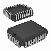
CY7B9911-5JCT Cypress Semiconductor Corp, CY7B9911-5JCT Datasheet - Page 12

CY7B9911-5JCT
Manufacturer Part Number
CY7B9911-5JCT
Description
IC CLK BUFF SKEW 8OUT 32PLCC
Manufacturer
Cypress Semiconductor Corp
Type
Fanout Distribution, Zero Delay Bufferr
Series
RoboClock+™r
Datasheet
1.CY7B9911-5JC.pdf
(15 pages)
Specifications of CY7B9911-5JCT
Number Of Circuits
1
Package / Case
32-PLCC
Pll
Yes
Input
TTL
Output
TTL
Ratio - Input:output
1:8
Differential - Input:output
No/No
Frequency - Max
100MHz
Divider/multiplier
Yes/Yes
Voltage - Supply
4.5 V ~ 5.5 V
Operating Temperature
0°C ~ 70°C
Mounting Type
Surface Mount
Frequency-max
100MHz
Output Frequency Range
3.75 MHz to 100 MHz
Supply Voltage (max)
5.5 V
Supply Voltage (min)
4.5 V
Maximum Operating Temperature
+ 70 C
Minimum Operating Temperature
0 C
Mounting Style
SMD/SMT
Operating Supply Voltage
5 V
Lead Free Status / RoHS Status
Contains lead / RoHS non-compliant
Available stocks
Company
Part Number
Manufacturer
Quantity
Price
Company:
Part Number:
CY7B9911-5JCT
Manufacturer:
Cypress
Quantity:
840
Company:
Part Number:
CY7B9911-5JCT
Manufacturer:
Cypress Semiconductor Corp
Quantity:
10 000
Figure 10
a zero-skew clock distribution tree between boards. Delays of
the downstream clock buffers are programmed to compensate
for the wire length (that is, select negative skew equal to the wire
delay) necessary to connect them to the master clock source,
Document Number: 38-07209 Rev. *F
DISTRIBUTION
SYSTEM
CLOCK
20 MHz
CLOCK
shows the CY7B9911 connected in series to construct
4F0
4F1
3F0
3F1
2F0
2F1
1F0
1F1
TEST
FB
REF
FS
FB
REF
FS
4F0
4F1
3F0
3F1
2F0
2F1
1F0
1F1
TEST
Figure 11. Board-to-Board Clock Distribution
4Q0
4Q1
3Q0
3Q1
2Q0
2Q1
1Q0
1Q1
4Q0
4Q1
3Q0
3Q1
2Q0
2Q1
1Q0
1Q1
Figure 10. Multi-Function Clock Driver
REF
REF
approximating a zero delay clock tree. Cascaded clock buffers
accumulate low frequency jitter because of the non-ideal filtering
characteristics of the PLL filter. Do not connect more than two
clock buffers in series.
SKEWED4ns
L4
80 MHz
L1
L2
ZEROSKEW
L3
INVERTED
80 MHz
20 MHz
80 MHz
Z
0
FB
REF
FS
4F0
4F1
3F0
3F1
2F0
2F1
1F0
1F1
TEST
Z
0
Z
Z
0
Z
Z
0
Z
0
Z
0
0
0
4Q0
4Q1
3Q0
3Q1
2Q0
2Q1
1Q0
1Q1
LOAD
LOAD
LOAD
LOAD
LOAD
LOAD
LOAD
RoboClock+™
CY7B9911
LOAD
Page 12 of 15
LOAD
[+] Feedback


