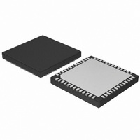
NB7N017MMNR2G ON Semiconductor, NB7N017MMNR2G Datasheet - Page 10

NB7N017MMNR2G
Manufacturer Part Number
NB7N017MMNR2G
Description
IC DIVIDER 8BIT DUAL CML 52-QFN
Manufacturer
ON Semiconductor
Type
Clock Dividerr
Datasheet
1.NB7N017MMNR2G.pdf
(19 pages)
Specifications of NB7N017MMNR2G
Pll
No
Input
CML, ECL, LVCMOS, LVDS, LVTTL
Output
CML
Number Of Circuits
1
Ratio - Input:output
1:1
Differential - Input:output
Yes/Yes
Frequency - Max
3.5GHz
Divider/multiplier
Yes/No
Voltage - Supply
±3 V ~ 3.465 V
Operating Temperature
-40°C ~ 85°C
Mounting Type
Surface Mount
Package / Case
52-VFQFN Exposed Pad
Frequency-max
3.5GHz
Mounting Style
SMD/SMT
Lead Free Status / RoHS Status
Lead free / RoHS Compliant
Available stocks
Company
Part Number
Manufacturer
Quantity
Price
Part Number:
NB7N017MMNR2G
Manufacturer:
ON/安森美
Quantity:
20 000
NOTE: Device will meet the specifications after thermal equilibrium has been established when mounted in a test socket or printed circuit
19. Measured using a 400 mV source, 50% duty cycle clock source at f
20. V
21. Device−to−Device skew for identical transitions at identical V
Table 11. AC CHARACTERISTICS
Symbol
V
t
t
t
V
t
t
t
t
t
t
t
PLH
PHL
JITTER
r
f
s
H
SKEW
PW
RR
OUTPP
INPP
rates 40 ps (20% − 80%).
INPP
,
board with maintained transverse airflow greater than 500 lfpm. Electrical parameters are guaranteed only over the declared operating
temperature range. Functional operation of the device exceeding these conditions is not implied. Device specification limit values are
applied individually under normal operating conditions and not valid simultaneously.
(MAX) cannot exceed V
Output Voltage Amplitude @ B 2 Mode
(See Figure 5)
Propagation Delay to Output Differential
RMS Random Clock Jitter f
(See Figure 5)
Input Voltage Swing/Sensitivity
(Differential Configuration) (Note 20)
Output Rise/Fall Times
(20% − 80%)
Setup Time
(Figure 23)
Hold Time
(Figure 23)
Minimum Pulse Width
Reset Recovery
Figure 5. Output Voltage Amplitude (V
Characteristic
Device−to−Device (Note 21)
CC
400
300
200
100
− V
0
in
MR to CLK/CLK
EE
CLK to PLb[7:0]
CLK to PLb[7:0]
Pa[7:0] to CLK
Pb[7:0] to CLK
0
= 3.5 GHz
V
Pa[7:0] to PLa
Pb[7:0] to PLb
PLa to Pa[7:0]
PLb to Pb[7:0]
.
f
CC
in
SEL to CLK
CLK to SEL
PLa to CLK
PLb to CLK
CLK to PLa
CLK to PLb
CE to CLK
CLK to CE
CLK to TC
= 3.5 GHz
MR to TC
= 0 V; V
0.5
@ Ambient Temperature (Typical)
MR
EE
INPUT FREQUENCY (MHz)
1
= −3.465 V to −3.0 V or V
−1500
−1250
−1750
−2250
−2250
−2000
3750
4500
2500
3250
4750
3000
3000
http://onsemi.com
Min
300
435
100
100
400
300
450
250
25
0
NB7N017M
1.5
CC
−40°C
levels.
OUTPP
−2700
−1900
−1900
−2700
−3200
−2500
2500
2000
2000
2750
3500
2500
2500
−110
in
Typ
400
120
V
45
30
40
40
85
10
RMS Jitter
= 1 GHz unless stated otherwise. All loading with 50 W to V
OUTPP
2
) / RMS Jitter vs. Input Frequency (f
2500
Max
555
500
2.5
65
75
2.5
CC
−1500
−1250
−1750
−2250
−2250
−2000
3750
4500
2500
3250
4750
3000
3000
3
= 3.0 V to 3.465 V; V
Min
300
455
100
100
400
300
450
250
25
0
3.5
−2700
−1900
−1900
−2700
−3200
−2500
25°C
2500
2000
2000
2750
3500
2500
2500
−110
Typ
400
120
45
30
40
40
85
4
4
3
2
1
0
2500
Max
575
500
3.0
65
75
EE =
0 V (Note 19)
−1500
−1250
−1750
−2250
−2250
−2000
3750
4500
2500
3250
4750
3000
3000
Min
300
475
100
100
400
300
450
250
25
0
in
)
−2700
−1900
−1900
−2700
−3200
−2500
85°C
2500
2000
2000
2750
3500
2500
−110
2500
Typ
400
120
45
30
40
40
85
CC
2500
. Input edge
Max
595
500
3.0
65
75
Unit
mV
mV
ps
ps
ps
ps
ps
ps
ps
ps


