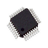
IDT5V9885PFGI IDT, Integrated Device Technology Inc, IDT5V9885PFGI Datasheet - Page 11

IDT5V9885PFGI
Manufacturer Part Number
IDT5V9885PFGI
Description
IC CLK GEN 3.3V EEPROM 32-TQFP
Manufacturer
IDT, Integrated Device Technology Inc
Type
Clock Generatorr
Datasheet
1.IDT5V9885NLGI.pdf
(37 pages)
Specifications of IDT5V9885PFGI
Pll
Yes with Bypass
Input
LVCMOS, LVTTL, Crystal
Output
LVCMOS, LVDS, LVPECL, LVTTL
Number Of Circuits
1
Ratio - Input:output
2:8
Differential - Input:output
No/Yes
Frequency - Max
500MHz
Divider/multiplier
Yes/Yes
Voltage - Supply
3.135 V ~ 3.6 V
Operating Temperature
-40°C ~ 85°C
Mounting Type
Surface Mount
Package / Case
32-TQFP, 32-VQFP
Frequency-max
500MHz
Number Of Elements
3
Supply Current
120mA
Pll Input Freq (min)
1MHz
Pll Input Freq (max)
400MHz
Operating Supply Voltage (typ)
3.3V
Operating Temp Range
-40C to 85C
Package Type
TQFP
Output Frequency Range
0.0049 to 500MHz
Operating Supply Voltage (min)
3V
Operating Supply Voltage (max)
3.6V
Operating Temperature Classification
Industrial
Pin Count
32
Lead Free Status / RoHS Status
Lead free / RoHS Compliant
Other names
5V9885PFGI
800-1992
IDT5V9885PFGI
800-1992
IDT5V9885PFGI
Available stocks
Company
Part Number
Manufacturer
Quantity
Price
Company:
Part Number:
IDT5V9885PFGI
Manufacturer:
IDT
Quantity:
513
Company:
Part Number:
IDT5V9885PFGI
Manufacturer:
IDT, Integrated Device Technology Inc
Quantity:
10 000
Part Number:
IDT5V9885PFGI
Manufacturer:
IDT
Quantity:
20 000
Company:
Part Number:
IDT5V9885PFGI8
Manufacturer:
IDT, Integrated Device Technology Inc
Quantity:
10 000
PLL is programmed for fractional divide.
TSSC > '0', SS_OFFSET = '0', and SD = '0' in order to prevent an unstable state in the modulator. The A[3:0] must be used and set to be greater than '2' for
a more accurate fractional divide.
IDT5V9885
3.3V EEPROM PROGRAMMABLE CLOCK GENERATOR
The spread spectrum parameters such as the modulation frequency and profile will not be enabled nor will it have any impact on the PLL output when the
The following is an example of how to set the fractional divider.
Example
F
Solving for 350MHz using Eq.2 and Eq.3 with PLL0 and spread spectrum off,
350MHz = 20MHz * (M / D)
For better jitter performance, keep D as small as possible
350MHz * 2 = M = 35
Therefore, we have D = 1, M = 35 (N = 16, A = 2) for PLL0 with P = 1 on output bank4 resulting in 350MHz.
Solving for 168.75MHz with PLL1 and fractional divide enabled:
168.75MHz = 20MHz * (M / D)
168.75MHz * 2 = M = 16.875 or 33.75
The 33.75 value is chosen to achieve the highest VCO frequency possible. Next step is to figure out the setting for the fractional divide using Eq.3.
33.75 = 2*N + A + 1 + SS_OFFSET * 1/64
Integer value 33 can be determined by N and A, thus leaving 0.75 left to be solved.
2*N + A + 1 = 33
SS_OFFSET = 64 * 0.75 = 48
Therefore, we have D=1, M=33.75 (N=15, A=2, SS_OFFSET=48) for PLL1 with P=2 on an output bank resulting in 168.75MHz.
The fractional divider can be determined if it is needed by following the steps in the previous example. Note that the 5v9885 should not be programmed with
IN
20MHz
= 20MHz, F
20MHz
P
OUT
P * 2
P
1 = 168.75MHz, F
P * 2
1
1
2
OUT
2 = 350MHz
11
INDUSTRIAL TEMPERATURE RANGE


