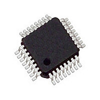
IDT5V9885PFGI IDT, Integrated Device Technology Inc, IDT5V9885PFGI Datasheet - Page 12

IDT5V9885PFGI
Manufacturer Part Number
IDT5V9885PFGI
Description
IC CLK GEN 3.3V EEPROM 32-TQFP
Manufacturer
IDT, Integrated Device Technology Inc
Type
Clock Generatorr
Datasheet
1.IDT5V9885NLGI.pdf
(37 pages)
Specifications of IDT5V9885PFGI
Pll
Yes with Bypass
Input
LVCMOS, LVTTL, Crystal
Output
LVCMOS, LVDS, LVPECL, LVTTL
Number Of Circuits
1
Ratio - Input:output
2:8
Differential - Input:output
No/Yes
Frequency - Max
500MHz
Divider/multiplier
Yes/Yes
Voltage - Supply
3.135 V ~ 3.6 V
Operating Temperature
-40°C ~ 85°C
Mounting Type
Surface Mount
Package / Case
32-TQFP, 32-VQFP
Frequency-max
500MHz
Number Of Elements
3
Supply Current
120mA
Pll Input Freq (min)
1MHz
Pll Input Freq (max)
400MHz
Operating Supply Voltage (typ)
3.3V
Operating Temp Range
-40C to 85C
Package Type
TQFP
Output Frequency Range
0.0049 to 500MHz
Operating Supply Voltage (min)
3V
Operating Supply Voltage (max)
3.6V
Operating Temperature Classification
Industrial
Pin Count
32
Lead Free Status / RoHS Status
Lead free / RoHS Compliant
Other names
5V9885PFGI
800-1992
IDT5V9885PFGI
800-1992
IDT5V9885PFGI
Available stocks
Company
Part Number
Manufacturer
Quantity
Price
Company:
Part Number:
IDT5V9885PFGI
Manufacturer:
IDT
Quantity:
513
Company:
Part Number:
IDT5V9885PFGI
Manufacturer:
IDT, Integrated Device Technology Inc
Quantity:
10 000
Part Number:
IDT5V9885PFGI
Manufacturer:
IDT
Quantity:
20 000
Company:
Part Number:
IDT5V9885PFGI8
Manufacturer:
IDT, Integrated Device Technology Inc
Quantity:
10 000
LOOP FILTER
the jitter transfer characteristics. The loop bandwidth can be extracted from the jitter transfer. A narrow loop bandwidth is good for jitter attenuation while a wide
loop bandwidth is best for low jitter generation. The specific loop filter components that can be programmed are the resistor via the RZ[3:0] bits, pole capacitor
via the CZ[3:0] bits, zero capacitor via the CP[3:0] bits, and the charge pump current via the IP[2:0] bits.
the fastest and easiest way to calculate the PLL loop bandwidth (Fc) given the programmable loop filter parameters is as follows.
phase margin thus compromising loop stability.
IDT5V9885
3.3V EEPROM PROGRAMMABLE CLOCK GENERATOR
The loop filter for each PLL can be programmed to optimize the jitter performance. The low-pass frequency response of the PLL is the mechanism that dictates
The following equations govern how the loop filter is set.
Resistor (Rz) = 0.3KΩ + RZ[3:0] * 1KΩ
Zero capacitor (Cz) = 6pF + CZ[3:0] * 27.2pF (Eq. 16)
Pole capacitor (Cp) = 1.3pF + CP[3:0] * 0.75pF (Eq. 17)
Charge pump current (Ip) = 5 * 2
PLL loop filter design is beyond the scope of this datasheet. Refer to design procedures for 3-order charge-pump based PLLs. For the sake of simplicity,
PLL Loop Bandwidth:
Charge pump gain (Kφ) = Ip / 2π
VCO gain (K
M = Total multiplier value (See the PRE-SCALERS, FEEDBACK-DIVIDERS, POST-DIVIDERS section for more detail)
ωc = Rz * Kφ * K
Fc = ωc / 2π
Note, the phase/frequency detector frequency (F
Parameter
C P
CZ
RZ
IP
M * (Cz + Cp)
VCO
) = 950MHz/V * 2π (Eq. 20)
VCO
* Cz (Eq. 21)
(Eq. 22)
Bits
4
4
4
3
IP[2:0]
From PFD
μA
(Eq. 19)
DOWN
(Eq. 15)
(Eq. 18)
Charge Pump and Loop Filter Configuration
PFD
UP
) is typically seven times the PLL closed-loop bandwidth (Fc) but too high of a ratio will reduce your
Step
27.2
0.75
2
1
n
V
DD
Ip
Ip
12
Min
0.3
1.3
6
5
Cz
Rz
Cp
To VCO
INDUSTRIAL TEMPERATURE RANGE
12.55
Max
15.3
414
640
Units
K Ω
μA
pF
pF


