LMX2353SLBX National Semiconductor, LMX2353SLBX Datasheet - Page 11
LMX2353SLBX
Manufacturer Part Number
LMX2353SLBX
Description
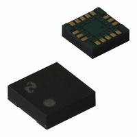
IC FREQ SYNTH 2.5GHZ 16LAMCSP
Manufacturer
National Semiconductor
Series
PLLatinum™r
Type
PLL Frequency Synthesizerr
Datasheet
1.LMX2353TMNOPB.pdf
(19 pages)
Specifications of LMX2353SLBX
Pll
Yes with Bypass
Input
CMOS, TTL
Output
CMOS
Number Of Circuits
1
Ratio - Input:output
2:1
Differential - Input:output
Yes/No
Frequency - Max
2.5GHz
Divider/multiplier
Yes/Yes
Voltage - Supply
2.7 V ~ 5.5 V
Operating Temperature
-40°C ~ 85°C
Mounting Type
Surface Mount
Package / Case
16-Laminate CSP
Frequency-max
2.5GHz
Lead Free Status / RoHS Status
Lead free / RoHS Compliant
Other names
LMX2353SLBX/NOPB
LMX2353SLBXTR
LMX2353SLBXTR
Available stocks
Company
Part Number
Manufacturer
Quantity
Price
Company:

Part Number:
LMX2353SLBX
Manufacturer:
ON
Quantity:
100


Most Significant Bit
MODE
DLL_
_21
23
2.0 Programming Description
2.2 R REGISTER
If the ADDRESS[1:0] field is set to 1 0 data is transferred from the 24-bit shift register into the R register which sets the PLL’ s
15-bit R-counter divide ratio when Latch Enable (LE) signal goes high. The divide ratio is put into the R_CNTR[14:0] field and is
described in section 2.2.1. The divider ratio must be
(DLL_MODE), Charge Pump (CP_WORD) are detailed in section 2.2.2 -2.2.4 below.
Note: R-counter divide ratio must be from 3 to 32,767.
2.2.2 V2_EN (R_20)
The V2_EN bit when set high enables the voltage doubler for the charge pump supply.
2.2.3 DLL_MODE (R_21)
The DLL_MODE bit should be set to 1 for normal usage.
2.2.4 CP_WORD (R_15-R_19)
2.2.4.1 Charge Pump Output Truth Table
R
2.2.1 Reference Divide Ratio (R_CNTR)
If the ADDRESS [1:0] field is set to 1 0 data is transferred MSB first from the 24-bit shift register into a latch which sets the 15-bit
R Counter, R_CNTR[14:0]. Serial data format is shown below.
Divide Ratio
32,767
V2_
_20
EN
V2_EN
22
R
3
4
DLL_MODE
•
ICP
CP_8X
Bit
R_19
O
Bit
_19
21
1600
R
100
200
300
400
900
µA (typ)
-
-
CP_WORD[4:0]
_18
20
R
R_14 R_13 R_12 R_11 R_10
0
0
1
•
_17
19
R
Location
_16
18
R_20
0
0
1
R
•
CP_4X
R_18
_15
Location
17
R
0
0
1
R_21
•
CP_8X
R_19
_14
16
R
0
0
0
0
1
1
-
-
0
0
1
•
_13
15
R
Data Field
(Continued)
Voltage Doubler Enable
_12
0
0
1
•
14
R
3. The bits used to control the voltage doubler (V2_EN), Delay Lock Loop,
SHIFT REGISTER BIT LOCATION
_11
R_9
13
Function
CP_2X
R
0
0
1
R_17
•
Calibration Mode
Delay Line Loop
11
CP_4X
_10
12
R_18
Function
R
R_8
0
0
0
0
0
1
-
-
0
0
1
•
R_CNTR[14:0]
R_CNTR[14:0]
11 10
_9
R
R_7
_8
R
0
0
1
•
_7
R
9
R_6
0
0
1
•
_6
R
8
CP_1X
R_16
_5
CP_2X
R
R_5
7
R_17
0
0
1
•
Disable
0
0
1
1
0
1
-
-
_4
R
6
0
Slow
R_4
0
_3
0
0
1
•
R
5
_2
R
4
R_3
0
0
1
•
_1
R
3
Least Significant Bit
PD_POL
R_2
_0
R
2
R_15
0
1
1
•
CP_1X
Enabled
R_16
0
1
0
1
0
1
-
-
Address Field
Fast
1
www.national.com
1
1
1
R_1
1
0
1
•
R_0
0
0
1
0
1
•
Related parts for LMX2353SLBX
Image
Part Number
Description
Manufacturer
Datasheet
Request
R

Part Number:
Description:
Pllatinum? Fractional N Single 2.5 Ghz Low Power Frequency Synthesizer
Manufacturer:
National Semiconductor Corporation
Datasheet:

Part Number:
Description:
National Semiconductor [8-Bit D/A Converter]
Manufacturer:
National Semiconductor
Datasheet:
Part Number:
Description:
National Semiconductor [Media Coprocessor]
Manufacturer:
National Semiconductor
Datasheet:
Part Number:
Description:
Digitally Controlled Tone and Volume Circuit with Stereo Audio Power Amplifier, Microphone Preamp Stage and National 3D Sound
Manufacturer:
National Semiconductor
Datasheet:
Part Number:
Description:
Digitally Controlled Tone and Volume Circuit with Stereo Audio Power Amplifier, Microphone Preamp Stage and National 3D Sound
Manufacturer:
National Semiconductor
Datasheet:
Part Number:
Description:
AC97 Rev 2 Codec with Sample Rate Conversion and National 3D Sound
Manufacturer:
National Semiconductor
Part Number:
Description:
Manufacturer:
National Semiconductor
Datasheet:
Part Number:
Description:
Manufacturer:
National Semiconductor
Datasheet:
Part Number:
Description:
General Purpose, Low Voltage, Low Power, Rail-to-Rail Output Operational Amplifiers
Manufacturer:
National Semiconductor
Datasheet:
Part Number:
Description:
8-bit 20 MSPS flash A/D converter.
Manufacturer:
National Semiconductor
Datasheet:
Part Number:
Description:
Low Noise Quad Operational Amplifier
Manufacturer:
National Semiconductor
Datasheet:
Part Number:
Description:
Quad Differential Line Receivers
Manufacturer:
National Semiconductor
Datasheet:
Part Number:
Description:
Quad High Speed Trapezoidal? Bus Transceiver
Manufacturer:
National Semiconductor
Datasheet:
Part Number:
Description:
Dual Line Receiver
Manufacturer:
National Semiconductor
Datasheet: