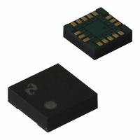
LMX2353SLBX National Semiconductor, LMX2353SLBX Datasheet - Page 8

LMX2353SLBX
Manufacturer Part Number
LMX2353SLBX
Description
IC FREQ SYNTH 2.5GHZ 16LAMCSP
Manufacturer
National Semiconductor
Series
PLLatinum™r
Type
PLL Frequency Synthesizerr
Datasheet
1.LMX2353TMNOPB.pdf
(19 pages)
Specifications of LMX2353SLBX
Pll
Yes with Bypass
Input
CMOS, TTL
Output
CMOS
Number Of Circuits
1
Ratio - Input:output
2:1
Differential - Input:output
Yes/No
Frequency - Max
2.5GHz
Divider/multiplier
Yes/Yes
Voltage - Supply
2.7 V ~ 5.5 V
Operating Temperature
-40°C ~ 85°C
Mounting Type
Surface Mount
Package / Case
16-Laminate CSP
Frequency-max
2.5GHz
Lead Free Status / RoHS Status
Lead free / RoHS Compliant
Other names
LMX2353SLBX/NOPB
LMX2353SLBXTR
LMX2353SLBXTR
Available stocks
Company
Part Number
Manufacturer
Quantity
Price
Company:
Part Number:
LMX2353SLBX
Manufacturer:
ON
Quantity:
100
www.national.com
1.0 Functional Description
increased while maintaining the same frequency step size for channel selection. The division value N is thereby reduced giving
a lower phase noise referred to the phase detector input, and the comparison frequency is increased allowing faster switching
times.
1.1 REFERENCE OSCILLATOR INPUT
The reference oscillator frequency for the PLL is provided by an external reference TCXO through the OSC
can operate to 50 MHz with a minimum input sensitivity of 0.5 V
from an external CMOS or TTL logic gate.
1.2 REFERENCE DIVIDER (R-COUNTER)
The R-counter is clocked through the oscillator block. The maximum frequency is 50 MHz. The R-counter is CMOS design and
15-bit in length with programmable divider ratio from 3 to 32,767.
1.3 FEEDBACK DIVIDER (N-COUNTER)
The N counter is clocked by the small signal f
The integer part is configured as a 5-bit A counter and a 10-bit B counter. The LMX2353 is capable of operating from 500 MHz
to 1.2 GHz with the 16/17 prescaler offering a continuous integer divide range from 272 to 16399, and 1.2 GHz to 2.5 GHz with
the 32/33 prescaler offering a continuous integer divide range from 1056 to 32767. The fractional compensation is programmable
in either 1/15 or 1/16 modes.
1.3.1 Prescaler
The RF input to the prescaler consist of f
complimentary input is internally coupled to ground with a 100 pF capacitor. This input is typically AC coupled to ground through
external capacitors as well. A 16/17 or 32/33 prescaler ratio can be selected.
1.3.2 Fractional Compensation
The fractional compensation circuitry in the N divider allows the user to adjust the VCO’s tuning resolution in 1/16 or 1/15
increments of the phase detector comparison frequency. A 4-bit register is programmed with the fractions desired numerator,
while another bit selects between fractional 15 and 16 modulo base denominator. An integer average is accomplished by using
a 4-bit accumulator. A variable phase delay stage compensates for the accumulated integer phase error, minimizing the charge
pump duty cycle, and reducing spurious levels. This technique eliminates the need for compensation current injection in to the
loop filter. Overflow signals generated by the accumulator are equivalent to 1 full VCO cycle, and result in a pulse swallow.
1.4 PHASE/FREQUENCY DETECTOR
The phase/frequency detector is driven from the N and R counter outputs. The maximum frequency at the phase detector input
is about 10 MHz for some high frequency VCO due to the minimum continuous divide ratio of the dual modulus prescaler. If the
phase detector frequency exceeds 2.37 MHz, there are higher chances of running into illegal divide ratios, because the minimum
continuous divide ratio with a 32/33 prescaler is 1056. The phase detector outputs control the charge pumps. The polarity of the
pump-up or pump-down control is programmed using PD_POL depending on whether the VCO characteristics are positive or
negative. The phase detector also receives a feedback signal from the charge pump, in order to eliminate dead zone.
1.5 CHARGE PUMPS
The phase detector’s current source output pumps charge into an external loop filter, which then integrates into the VCO’s control
voltage. The charge pump steers the charge pump output CP
primarily in a TRISTATE mode with small corrections. The charge pump output current magnitude can be selected from 100 µA
to 1.6 mA by programming the CP_WORD bits.
1.6 VOLTAGE DOUBLER
The V
pump circuit. An internal voltage doubler circuit connected between the V
(
enabled by setting the V2_EN bit (R[20]) to a HIGH level. The average delivery current of the doubler is less than the
instantaneous current demand of the RF charge pump when active and is thus not capable of sustaining a continuous out of lock
condition. A large external capacitor connected to V
frequencies.
1.7 MICROWIRE
The programmable functions are accessed through the MICROWIRE serial interface. The interface is made of three functions:
clock, data and latch enable (LE). Serial data for the various counters is clocked in from data on the rising edge of clock, into the
24-bit shift register. Data is entered MSB first. The last two bits decode the internal register address. On the rising edge of LE,
data stored in the shift register is loaded into one of the 4 appropriate latches (selected by address bits). A complete programming
description is included in the following sections.
±
10%) users to run the RF charge pump circuit at close to twice the V
p
pin is normally driven from an external power supply over a range of V
™
SERIAL INTERFACE
IN
IN
(Continued)
input pin. The N counter is 19 bits with 15 bits integer divide and 4 bits fractional.
and f
p
( 0.1 µF) is therefore needed to control power supply droop when changing
INB
; which are complimentary inputs to a differential pair amplifier. The
o
to V
8
pp
. The inputs have a V
CC
(pump-up) or Ground (pump-down). When locked, CP
CC
CC
power supply voltage. The Voltage doubler mode is
and V
CC
to 5.5V to provide current for the RF charge
p
supply pins alternately allows V
CC
/2 input threshold and can be driven
IN
pin. OSC
CC
IN
block
= 3V
o
is


