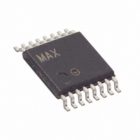
DS1123LE-25+ Maxim Integrated Products, DS1123LE-25+ Datasheet - Page 9

DS1123LE-25+
Manufacturer Part Number
DS1123LE-25+
Description
IC TIMING ELEMENT PROG 16-TSSOP
Manufacturer
Maxim Integrated Products
Datasheet
1.DS1123LE-200.pdf
(14 pages)
Specifications of DS1123LE-25+
Number Of Taps/steps
256
Function
Programmable
Delay To 1st Tap
16.5nS
Tap Increment
0.25nS
Available Total Delays
63.75ns
Voltage - Supply
3 V ~ 3.6 V
Operating Temperature
0°C ~ 70°C
Mounting Type
Surface Mount
Package / Case
16-TSSOP
Lead Free Status / RoHS Status
Lead free / RoHS Compliant
Number Of Independent Delays
-
effect on power-up. The most flexibility when using par-
allel mode occurs when the delay is being controlled
by a microprocessor.
There are two common parallel interface implementa-
tions used to control the DS1123L using a microproces-
sor (see Figure 2). LE can be used to latch the data
from the microprocessor, which allows the data bus to
be shared with other peripherals, or LE can be tied
Figure 2. Parallel Interface Options for DS1123L
Figure 4. Latched Parallel Timing Diagram
MICROPROCESSOR
MICROPROCESSOR
A) SHARING THE PARALLEL INTERFACE
B) A PARALLEL INTERFACE DEDICATED
TO A DS1123L
WITH ADDITIONAL PERIPHERALS
PARALLEL
ENABLE
3.3V, 8-Bit, Programmable Timing Element
INPUTS
PO–P7
DELAY
TIME
(LE)
V
CC
8
8
PREVIOUS VALUE
LE
P0-P7
LE
P0-P7
ADDITIONAL
PERIPHERAL
PERIPHERAL
ADDITIONAL
DS1123L
DS1123L
_____________________________________________________________________
P/S
P/S
t
EDX
t
EW
NEW VALUE
high, which causes the DS1123L to adjust its delay
immediately following a change to the parallel inputs.
For each configuration, a settling time (t
required after an adjustment is made before the input
signal is accurately delayed according to the new set-
ting. Figures 3 and 4 show the timing required for these
implementations.
The 3-wire serial interface is enabled by connecting P/S
to V
When LE is set at a high logic level, it enables the reg-
ister and CLK clocks the data, D, into the register one
bit at a time starting with the most significant bit. After
all 8 bits are shifted into the DS1123L, LE is pulled low
to end the data transfer and activate the new value. A
settling time (t
before the signal delay meets its specified accuracy. A
timing diagram for the serial interface is shown in
Figure 6. The 3-wire interface also has an output (Q)
that can be used to cascade multiple 3-wire devices,
and it can be used to read the current value of the
devices on the bus.
t
Figure 3. Nonlatched Parallel Timing Diagram
DSE
PARALLEL
INPUTS
P0–P7
DELAY
CC
Using the Serial Programming Interface
TIME
. Serial mode operates similar to a shift register.
PREVIOUS VALUE
PREVIOUS VALUE
EDV
t
EDV
t
PDX
) is required after LE is pulled low
t
DHE
NEW VALUE
EDV
NEW VALUE
or t
t
PDV
NEW VALUE
PDV
) is
9


