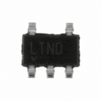
LTC1799CS5#TRMPBF Linear Technology, LTC1799CS5#TRMPBF Datasheet - Page 5

LTC1799CS5#TRMPBF
Manufacturer Part Number
LTC1799CS5#TRMPBF
Description
IC OSCILLATOR RES SET TSOT23-5
Manufacturer
Linear Technology
Type
Oscillator, Siliconr
Datasheet
1.LTC1799CS5TRMPBF.pdf
(14 pages)
Specifications of LTC1799CS5#TRMPBF
Frequency
33MHz
Voltage - Supply
2.7 V ~ 5.5 V
Current - Supply
7mA
Operating Temperature
0°C ~ 70°C
Package / Case
TSOT-23-5, TSOT-5, TSOP-5
Clock External Input
No
Supply Voltage Range
2.7V To 5.5V
Digital Ic Case Style
TSOT-23
No. Of Pins
5
Operating Temperature Range
0°C To +70°C
Msl
MSL 1 - Unlimited
Rohs Compliant
Yes
Lead Free Status / RoHS Status
Lead free / RoHS Compliant
Count
-
Other names
LTC1799CS5#TRMPBFTR
Available stocks
Company
Part Number
Manufacturer
Quantity
Price
pin FuncTions
V
ply must be kept free from noise and ripple. It should be
bypassed directly to a ground plane with a 0.1µF capacitor.
GND (Pin 2): Ground. Should be tied to a ground plane
for best performance.
SET (Pin 3): Frequency-Setting Resistor Input. The value
of the resistor connected between this pin and V
mines the oscillator frequency. The voltage on this pin is
held by the LTC1799 to approximately 1.13V below the
V
film resistor with a value between 10k and 200k and limit
the capacitance on this pin to less than 10pF .
DIV (Pin 4): Divider-Setting Input. This three-state input
selects among three divider settings, determining the
value of N in the frequency equation. Pin 4 should be tied
to GND for the ÷1 setting, the highest frequency range.
block DiagraM
+
+
(Pin 1): Voltage Supply (2.7V ≤ V
voltage. For best performance, use a precision metal
R
I
RES
SET
1
3
2
GND
V
SET
+
+
–
V
BIAS
I
RES
+
–
GAIN = 1
+
≤ 5.5V). This sup-
V
RES
(V
= 1.13V ±25%
+
– V
SET
+
)
deter-
ƒ
MO
= 100MHz • kΩ •
MASTER OSCILLATOR
Floating Pin 4 divides the master oscillator by 10. Pin 4
should be tied to V
quency range. To detect a floating DIV pin, the LTC1799
attempts to pull the pin toward midsupply. This is realized
with two internal current sources, one tied to V
4 and the other one tied to ground and Pin 4. Therefore,
driving the DIV pin high requires sourcing approximately
5µA. Likewise, driving DIV low requires sinking 5µA.
When Pin 4 is floated, preferably it should be bypassed
by a 1nF capacitor to ground or it should be surrounded
by a ground shield to prevent excessive coupling from
other PCB traces.
OUT (Pin 5): Oscillator Output. This pin can drive 5kΩ
and/or 10pF loads. Larger loads may cause inaccuracies
due to supply bounce at high frequencies. Transients will
not cause latchup if the current into/out of the OUT pin is
limited to 50mA.
(V
+
I
– V
RES
SET
)
+
DIVIDER
SELECT
PROGRAMMABLE
for the ÷100 setting, the lowest fre-
(÷1, 10 OR 100)
INPUT DETECT
THREE-STATE
DIVIDER
GND
OUT
DIV
5µA
5µA
LTC1799
1799 BD
V
+
5
4
+
and Pin
1799fc
5


